 | –≠–ª–µ–∫—Ç—Ä–æ–Ω–Ω—ã–π –∫–æ–º–ø–æ–Ω–µ–Ω—Ç: HT0638 | –°–∫–∞—á–∞—Ç—å:  PDF PDF  ZIP ZIP |
1
HT0638
HT0638
Electronic Line Switch
General Description
The Supertex HT0638 is an integrated electronic line switch
controllable from four logic-level inputs. These devices are
intended as a replacement for mechanical hook switches and
relays in telephones, answering machines, and similar telecom-
munications equipment. They switch the positive (Tip) side of the
telephone line using control inputs that are referenced to the
negative (Ring) side of the line. In the off state, it can hold-off 375
volts. In the on state, the series resistance is 15
maximum.
These devices provide adjustable current limiting via an external
sense resistor. Three of the control inputs are general purpose
and one is an override input that forces the switch to an off state
regardless of the state of the other inputs. This override input is
useful for `flash' and pulse dialing purposes. Internal pull-up/
down resistors allow the inputs to be driven from single-ended
sources, push-pull sources, or left unconnected.
The HT0638 is powered from the phone line and are especially
useful in applications where external power is not available. Due
to their low quiescent current, both of these devices exceed the
on-hook resistance requirements of EIA-470-A.
Features
15
maximum switch resistance
Current limiting protection
4 logic control inputs
Operates at 2V input
2
µ
A maximum quiescent current at 100V
Applications
Telephone handsets
Fax machines
Answering machines
Auto-dial alarm systems
08/23/02
Supertex Inc. does not recommend the use of its products in life support applications and will not knowingly sell its products for use in such applications unless it receives an adequate "products liability
indemnification insurance agreement." Supertex does not assume responsibility for use of devices described and limits its liability to the replacement of devices determined to be defective due to
workmanship. No responsibility is assumed for possible omissions or inaccuracies. Circuitry and specifications are subject to change without notice. For the latest product specifications, refer to the
Supertex website: http://www.supertex.com. For complete liability information on all Supertex products, refer to the most current databook or to the Legal/Disclaimer page on the Supertex website.
For additional information, refer to application note
AN-H32.
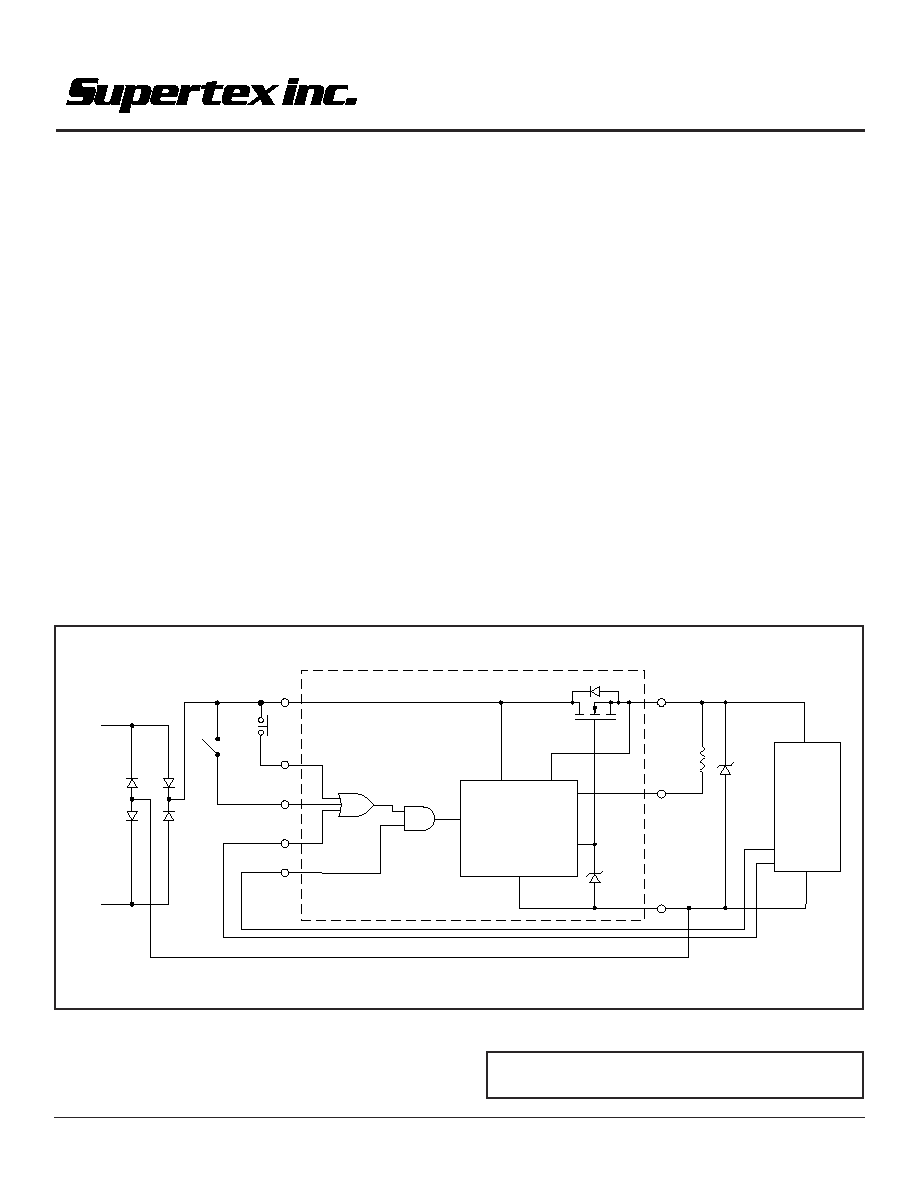
Typical Application Circuit
Low
Voltage
Telecom
IC
TPG
HT0640
TP
CS
GND
HKS
LS1
LS2
DP
H = ON
L = OFF
Charge Pump
&
Logic Control
+
15V
-
Tip
Ring
2
HT0638
Absolute Maximum Ratings
V
TPG
, Input line voltage
+375V
V
TP
, Output line voltage
+18V
HKS continuous input voltage
V
TPG
LS1, LS2 continuous input voltage
+20V
DP continuous input voltage
+5V
Storage temperature
≠65
∞
C to +150
∞
C
Soldering temperature*
+300
∞
C
Notes: All voltages are referenced to ground.
*Distance of 1.6mm from case for 10 seconds.
Ordering Information
Breakdown Voltage
Switch Resistance
Package Option
SO-8
375V
15
HT0638LG
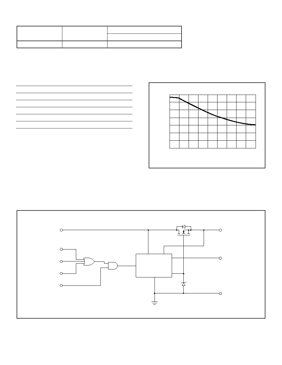
Typical Performance Curve
350
300
250
200
150
100
50
0
100
200 300
400 500
R
SENSE
(ohms)
I
LIMIT
vs. R
SENSE
600 700
800
900 1000
I
LIMIT
(mA)
Block Diagram
TPG
TP
CS
GND
HKS
LS1
LS2
DP
H = ON
L = OFF
Charge Pump
&
Logic Control
3
HT0638
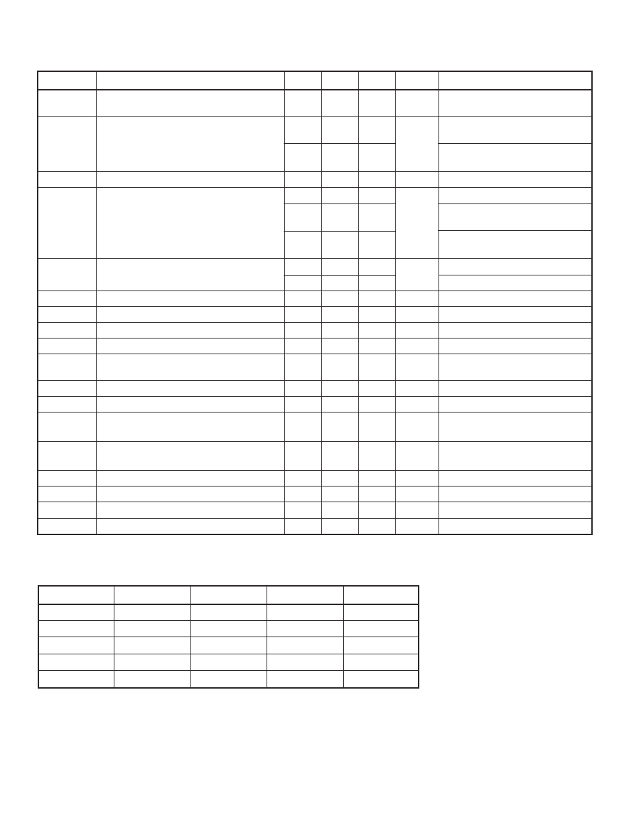
Truth Table
HKS
LS1
LS2
DP
Switch State
X
X
H
H or Z
ON
X
H
X
H or Z
ON
H
X
X
H or Z
ON
L or Z
L or Z
L or Z
X
OFF
X
X
X
L
OFF
Z = high impedance, open circuit
X = don't care
L = logic level low
H = logic level high
Symbol
Parameter
Min
Typ
Max
Unit
Conditions
V
TPG
High voltage positive supply
375
V
I
TP
= 10
µ
A, HKS, LS1, LS2,
DP = open circuit
I
TPQ
Input leakage current
2.0
µ
A
V
TPG
= 100V, HKS, LS1, LS2,
DP = open circuit
10
V
TPG
= 375V, HKS, LS1, LS2,
DP = open circuit
V
TP
Output voltage
16
18
20
V
V
TPG
= 50V, No Load
R
SW
TPG to TP switch resistance
15
V
TPG
=4.3V, I
TPG
=180mA, SW= On
15
V
TPG
=3.0V, I
TPG
=20mA, SW= On,
T
A
=0
∞
C to 50
∞
C
30
V
TPG
=2.0V, I
TPG
=5mA, SW= On
T
A
=0
∞
C to 50
∞
C
I
TPG
-I
TP
Bias current
50
µ
A
V
TPG
= 5.0V, SW = On
100
V
TPG
= 10V, SW = On
I
LIM
I
TPG
current limiting
200
300
mA
R
EXT
= 430
I
HKS
HKS input current
200
µ
A
V
HKS
= 50V
I
LS1
LS1 input current
136
µ
A
V
LS1
= 3.0V, V
DP
= 0V
I
LS2
LS2 input current
136
µ
A
V
LS2
= 3.0V, V
DP
= 0V
I
DP
DP output current
500
µ
A
V
DP
= 0V, V
HKS
= 50V,
V
LS1
=V
LS2
= 3.0V
V
IL(HKS)
HKS input low
0
0.2
V
V
IH(HKS)
HKS input high
2.0
V
TPG
V
V
IL(LS1)
,
LS1 and LS2 input low
0
0.2
V
V
IL(LS2)
V
IH(LS1)
,
LS1 and LS2 input high
1.0
20
V
V
IH(LS2)
V
IL(DP)
DP input low
0
0.2
V
V
IH(DP)
DP input high
1.0
5.0
V
T
ON
Turn on time
1.0
ms
V
TPG
= 4.5V
T
OFF
Turn off time
1.0
ms
V
TPG
= 4.5V
Electrical Characteristics
(over operating supply voltages unless otherwise specified, T
A
= -40
∞
C to +85
∞
C)
4
HT0638
1235 Bordeaux Drive, Sunnyvale, CA 94089
TEL: (408) 744-0100 ∑ FAX: (408) 222-4895
www.supertex.com
08/23/02
©2002 Supertex Inc. All rights reserved. Unauthorized use or reproduction prohibited.
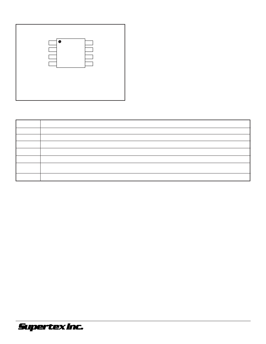
Pin Description
TPG
Positive input side of a telephone line, typically Tip side.
TP
Positive output side of a telephone line.
HKS
Hookswitch input. Connect HKS to TPG to turn on the electronic switch. Internally pulled low.
LS1
Line switch 1 input. Positive input turns on the electronic switch. Internally pulled low.
LS2
Line switch 2 input. Positive input turns on the electronic switch. Internally pulled low.
DP
Dial pulse input. A low input turns off the electronic switch. Use for pulse dialing. Internally pulled high.
CS
Current sense input. An external resistor connected between CS and TP sets the current limit. Short C
S
to TP if
current limiting is not used.
GND
Device ground. Negative side of a telephone line, typically Ring side.
1
2
3
4
8
7
6
5
Pin Configuration
TPG
TP
HKS
CS
GND
DP
LS2
LS1
Note: See Package Outline section for dimensions.
top view
SO-8