 | –≠–ª–µ–∫—Ç—Ä–æ–Ω–Ω—ã–π –∫–æ–º–ø–æ–Ω–µ–Ω—Ç: HT18LG | –°–∫–∞—á–∞—Ç—å:  PDF PDF  ZIP ZIP |

1
HT18
HT19
Electronic Telephone Line Switch
General Description
The Supertex HT18LG and HT19LG are electronic line switch
circuits that replace the mechanical hook switch contact or a
discrete hook switch in a telephone handset or modem. They
switch the positive side of the telephone line using control inputs
that are referenced to the negative side of the line. In the off state,
they can withstand 350V on the positive input. In the on state
their series resistances are 18 maximum. The devices provide
current limiting determined by an external resistor. There are
three control inputs. The HKS pin turns on the hook switch when
connected to the TPG pin. This can be accomplished by using a
mechanical switch which closes when the handset is physically
off-hook. The LS pin allows a logic signal to turn on the hook
switch. The dial pulse, Pin 6, is used to turn the hook switch off
for pulse dialing. For the HT18, the dial pulse is active high (DP)
whereas for the HT19, it is active low (DP).
Features
350V breakdown voltage
18 maximum switch resistance
Current limiting protection
Operates at 2.0V input
Applications
Telephone handsets
Modems
Fax machines
Answering machines
Remote meter reading
Phone interface products
Absolute Maximum Ratings
V
TPG
, Input line voltage
+350V
V
TP
, Output line voltage
+18V
DP/DP continuous input voltage
+10V
Storage temperature
≠65∞C to +150∞C
Junction temperature
+150∞C
Soldering temperature*
+300∞C
Power dissipation
0.8 Watt
Notes: All voltages are referenced to ground.
*Distance of 1.6mm from case for 10 seconds.
1
2
3
4
8
7
6
5
Pin Configuration
TPG
TP
HKS
CS
GND
DP/DP *
N/C
LS
Note: See Package Outline section for dimensions.
top view
SO-8
Package Option
Dial Pulse Pin
SO-8
Breakdown Voltage
Switch Resistance
DP/DP
350V
18
Active High
HT18LG
350V
18
Active Low
HT19LG
Ordering Information
* For HT18, Pin 6 is DP.
For HT19, Pin 6 is DP.
12/13/01
Supertex Inc. does not recommend the use of its products in life support applications and will not knowingly sell its products for use in such applications unless it receives an adequate "products liability
indemnification insurance agreement." Supertex does not assume responsibility for use of devices described and limits its liability to the replacement of devices determined to be defective due to
workmanship. No responsibility is assumed for possible omissions or inaccuracies. Circuitry and specifications are subject to change without notice. For the latest product specifications, refer to the
Supertex website: http://www.supertex.com. For complete liability information on all Supertex products, refer to the most current databook or to the Legal/Disclaimer page on the Supertex website.
2
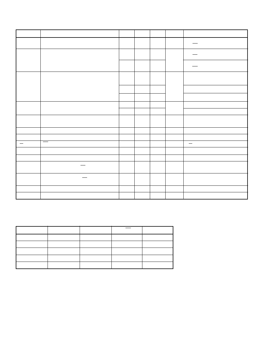
Symbol
Parameter
Min
Typ
Max
Unit
Conditions
V
TPG
High voltage positive supply
350
V
I
TPG
= 500µA, HKS, LS,
DP/DP = open circuit
I
TPG
Input leakage current
2.0
µA
V
TPG
= 100V, HKS, LS,
DP/DP = open circuit
V
TPG
= 290V, HKS, LS,
200
DP/DP = open circuit
R
SW
TPG to TP switch resistance
18
V
TPG
=17V, I
TPG
=180mA, SW= On
18
V
TPG
=3.0V, I
TPG
=20mA, SW= On
30
V
TPG
=2.0V, I
TPG
=5mA, SW= On
I
TPG
-I
TP
Bias current
50
µA
V
TPG
= 5.0V, SW = On
100
V
TPG
= 10V, SW = On
I
LIM
I
TPG
current limiting
188
250
313
mA
R
EXT
= 158 ± 1%
I
HKS
HKS input current
200
µA
V
HKS
= 40V to 70V
I
LS
, I
DP
LS and DP logic input current
30
µA
V
LS
= 3.0V, V
DP
= 3.0V
I
DP
DP logic input current
-30
µA
V
DP
= 0V
V
IL(HKS)
HKS input low
0
0.2
V
V
TPG
= 3.0V to 70V
V
IH(HKS)
HKS input high
2.0
V
TPG
V
V
TPG
= 3.0V to 70V
V
IL(LS)
,
Input logic low for DP/DP and LS
0
0.2
V
V
TPG
= 3.0V to 70V
V
IL(DP)
V
IH(LS)
,
Input logic high for DP/DP and LS
1.5
10
V
V
TPG
= 3.0V to 70V
V
IH(DP)
T
ON
Turn on time
1.0
ms
V
TPG
= 4.5V
T
OFF
Turn off time
1.0
ms
V
TPG
= 4.5V
Electrical Characteristics
(Over operating supply voltages unless otherwise specified, T
A
= 0∞C to +50∞C)
Truth Table
HKS
LS
DP
DP
Switch State
H
L or Z
L or Z
H or Z
ON
H
H
L or Z
H or Z
ON
L or Z
L or Z
L or Z
H or Z
OFF
L or Z
H
L or Z
H or Z
ON
X
X
H
L
OFF
Z = high impedance, open circuit
X = don't care
L = logic level low
H = logic level high
HT18/HT19

3
Block Diagram
TPG
TP
CS
GND
HKS
LS
DP
H = ON
L = OFF
Charge Pump
&
Logic Control
(1)
(2)
(5)
(6) for HT18
(6) for HT19
(8)
(7)
(3)
DP
Pin Description
Pin # Symb
Description
1
TPG
Positive input side of a telephone line, typically Tip side.
2
HKS
Hookswitch input. Connect HKS to TPG to turn on the hook switch. Internally pulled low with a high value resistor.
3
GND
Device ground. Negative side of a telephone line, typically Ring side.
4
NC
No Connect. Open Circuit. No internal connections to the device.
5
LS
Line switch input. Input logic high turns on the hook switch. Internally pulled low with a high value resistor.
6
DP
For HT18. Dial pulse input. Input logic high turns off the hook switch. Used for pulse dialing. Internally pulled low with a
high value resistor.
6
DP
For HT19. Dial pulse input. Input logic low turns off the hook switch. Used for pulse dialing. Internally pulled high with a
high value resistor.
7
CS
Current sense input. An external resistor connected between CS and TP sets the current limit.
8
TP
Positive output side of a telephone line. Zener protection to prevent this output from rising above 18V is required.
HT18/HT19
Typical Application Circuit
Tip
Ring
Transient
Protection
TPG
HKS
GND
DP/DP
LS
CS
R
SEN
15V
HT18
or
HT19
Telecom
Circuit
TP
1235 Bordeaux Drive, Sunnyvale, CA 94089
TEL: (408) 744-0100 ∑ FAX: (408) 222-4895
www.supertex.com
12/13/010
©2001 Supertex Inc. All rights reserved. Unauthorized use or reproduction prohibited.