
1
HV100/HV101
08/26/02
Supertex Inc. does not recommend the use of its products in life support applications and will not knowingly sell its products for use in such applications unless it receives an adequate "products liability
indemnification insurance agreement." Supertex does not assume responsibility for use of devices described and limits its liability to the replacement of devices determined to be defective due to
workmanship. No responsibility is assumed for possible omissions or inaccuracies. Circuitry and specifications are subject to change without notice. For the latest product specifications, refer to the
Supertex website: http://www.supertex.com. For complete liability information on all Supertex products, refer to the most current databook or to the Legal/Disclaimer page on the Supertex website.
HV100
HV101
Applications
-48V Central Office Switching (line cards)
+48V Server Networks
+48V Storage Area Networks
+48V Peripherals, Routers, Switches
+24V Cellular and Fixed Wireless (bay stations, line cards)
+24V Industrial Systems
+24V UPS Systems
-48V PBX & ADSL Systems (line cards)
Distributed Power Systems
Powered Ethernet for VoIP
Features
33% Smaller than SOT-23
2
Pass Element is Only External Part
No Sense Resistor required
Auto-Adapt* to Pass Element
Short Circuit Protection*
UV & POR Supervisory Circuits
2.5s Auto Retry
�
10V to
�
72V Input Voltage Range
0.6mA Typical Operating Supply Current
Built in Clamp for AC Path Turn On Glitch
Typical Applications and Waveforms
-48V
GND
GATE
V
PP
V
NN
HV100
DC/DC
Converter
+5V
COM
IRF530
400�F
General Description
The HV100/HV101 are 3-pin hotswap controllers available in
SOT-223 and MLP packages, which require no external compo-
nents other than a pass element. The HV100/HV101 contain
many of the features found in hotswap controllers with 8 pins or
more, and which generally require many external components.
These features include undervoltage (UV) detection circuits,
power on reset (POR) supervisory circuits, inrush current limit-
ing, short circuit protection, and auto-retry. In addition, the
HV100/HV101 use a patent pending mechanism to sample and
adapt to any pass element, resulting in consistent hotswap
profiles without any programming.
The only difference between the HV100 and the HV101 is the
internally set undervoltage (UV) threshold.
Ordering Information
V
U
s
n
o
i
t
p
O
s
n
o
i
t
p
O
e
g
a
k
c
a
P
3
2
2
-
T
O
S
n
i
P
-
3
P
L
M
n
i
P
-
3
e
i
D
V
4
3
5
K
0
0
1
V
H
6
K
0
0
1
V
H
X
0
0
1
V
H
V
4
1
5
K
1
0
1
V
H
6
K
1
0
1
V
H
X
1
0
1
V
H
*Patents Pending
1
IRF530 is a Trademark of International Rectifier Corporation
2
MLP3x2 Package Version compared to 3mmx3mm SOT-23-6
Demo Kit
Available
3-Pin Hotswap, Inrush Current Limiter Controllers
(Negative Supply Rail)
2
HV100/HV101
Electrical Characteristics
(-40
�
C < T
A
< +85
�
C unless otherwise noted)
l
o
b
m
y
S
r
e
t
e
m
a
r
a
P
n
i
M
p
y
T
x
a
M
s
t
i
n
U
s
n
o
i
t
i
d
n
o
C
y
l
p
p
u
S
V
o
t
d
e
c
n
e
r
e
f
e
R
(
P
P
)
n
i
p
V
N
N
e
g
a
t
l
o
V
y
l
p
p
u
S
2
7
-
V
U
V
I
N
N
t
n
e
r
r
u
C
y
l
p
p
u
S
6
.
0
0
.
1
A
m
V
N
N
V
8
4
-
=
l
o
r
t
n
o
C
V
U
V
o
t
d
e
c
n
e
r
e
f
e
R
(
N
N
)
n
i
p
V
L
V
U
)
w
o
L
o
t
h
g
i
H
(
d
l
o
h
s
e
r
h
T
V
U
0
3
4
3
8
3
V
0
0
1
V
H
3
.
2
1
4
1
7
.
5
1
V
1
0
1
V
H
V
H
V
U
s
i
s
e
r
e
t
s
y
H
V
U
3
V
0
0
1
V
H
1
V
1
0
1
V
H
t
u
p
t
u
O
e
v
i
r
D
e
t
a
G
V
o
t
d
e
c
n
e
r
e
f
e
R
(
N
N
)
n
i
p
V
E
T
A
G
e
g
a
t
l
o
V
e
v
i
r
D
e
t
a
G
m
u
m
i
x
a
M
0
1
2
1
4
1
V
R
S
E
T
A
G
e
t
a
R
w
e
l
S
l
a
i
t
i
n
I
5
7
.
1
5
.
2
5
2
.
3
s
m
/
V
C
E
T
A
G
F
n
1
=
I
N
W
O
D
E
T
A
G
)
g
n
i
k
n
i
s
(
t
n
e
r
r
u
C
n
w
o
D
-
ll
u
P
e
v
i
r
D
e
t
a
G
8
6
1
A
m
V
E
T
A
G
V
;
V
1
=
P
P
V
5
.
1
1
=
I
P
U
L
L
U
P
t
n
e
r
r
u
C
p
u
-
ll
u
P
p
a
w
S
t
o
H
t
s
o
P
6
1
1
A
�
V
E
T
A
G
V
6
=
l
o
r
t
n
o
C
g
n
i
m
i
T
V
o
t
d
e
c
n
e
r
e
f
e
R
(
N
N
)
n
i
p
t
R
O
P
y
a
l
e
D
R
O
P
n
o
i
t
r
e
s
n
I
5
.
1
5
.
3
5
.
5
s
m
t
D
R
A
y
a
l
e
D
t
r
a
t
s
e
R
o
t
u
A
5
2
.
1
5
.
2
5
7
.
3
s
s
t
l
u
s
e
R
l
a
c
i
r
t
c
e
l
E
e
l
p
m
a
x
E
)
0
3
5
F
R
I
g
n
i
s
U
(
I
M
I
L
p
a
w
s
t
o
H
g
n
i
r
u
D
t
n
e
r
r
u
C
h
s
u
r
n
I
x
a
M
4
.
1
A
C
,
T
E
F
S
O
M
l
a
n
r
e
t
x
e
0
3
5
F
R
I
D
A
O
L
F
�
0
0
1
=
I
M
I
L
p
a
w
s
t
o
H
g
n
i
r
u
D
t
n
e
r
r
u
C
h
s
u
r
n
I
x
a
M
5
.
2
A
C
,
T
E
F
S
O
M
l
a
n
r
e
t
x
e
0
3
5
F
R
I
D
A
O
L
F
�
0
0
2
=
I
M
I
L
p
a
w
s
t
o
H
g
n
i
r
u
D
t
n
e
r
r
u
C
h
s
u
r
n
I
x
a
M
1
.
3
A
C
,
T
E
F
S
O
M
l
a
n
r
e
t
x
e
0
3
5
F
R
I
D
A
O
L
F
�
0
0
3
=
I
T
R
O
H
S
t
r
o
h
S
a
o
t
n
I
t
n
e
r
r
u
C
x
a
M
0
.
4
A
R
,
T
E
F
S
O
M
l
a
n
r
e
t
x
e
0
3
5
F
R
I
D
A
O
L
1
<
<
=
t
T
R
O
H
S
e
m
i
T
c
e
t
e
D
d
a
o
L
d
e
t
r
o
h
S
0
.
1
s
m
R
,
T
E
F
S
O
M
l
a
n
r
e
t
x
e
0
3
5
F
R
I
D
A
O
L
1
<
<
=
E
T
A
G
e
t
a
G
f
o
e
s
i
R
f
o
e
t
a
R
l
a
i
t
i
n
I
5
.
2
s
m
/
V
C
y
n
a
,
T
E
F
S
O
M
l
a
n
r
e
t
x
e
0
3
5
F
R
I
D
A
O
L
t
S
H
e
g
a
t
l
o
V
e
t
a
G
ll
u
F
o
t
d
o
i
r
e
P
p
a
w
S
t
o
H
5
.
2
1
s
m
C
y
n
a
,
T
E
F
S
O
M
l
a
n
r
e
t
x
e
0
3
5
F
R
I
D
A
O
L
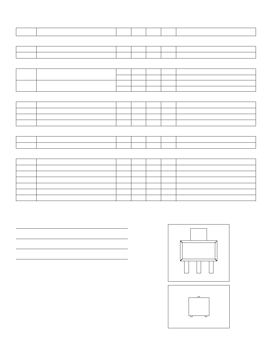
Pin Description
V
PP
� Positive voltage supply input to the circuit.
V
NN
� This pin is the Negative voltage power supply input to
the circuit.
GATE
� This is the Gate Driver Output for the external N-
Channel MOSFET.
Absolute Maximum Ratings*
V
PP
Input Voltage
-0.3V to 75V
Operating Ambient Temperature Range
-40
�
C to +85
�
C
Operating Junction Temperature Range
-40
�
C to 125
�
C
Storage Temperature Range
-65
�
C to 150
�
C
*All voltages referenced to V
NN
.
Pinouts
1
2
3
VNN
GATE
2
VPP
Top View
SOT-223
1
2
3
VPP
GATE
VNN
Top View
3 pin MLP

3
HV100/HV101
Functional Block Diagram
Regulator
UVLO
UV
POR
Timer
Reference
Generator
Logic
Restart
Timer
GATE
VPP
VNN
Functional Description
Insertion into Hot Backplanes
Telecom, data network and some computer applications require
the ability to insert and remove circuit cards from systems
without powering down the entire system. Since all circuit cards
have some filter capacitance on the power rails, which is espe-
cially true in circuit cards or network terminal equipment utilizing
distributed power systems, the insertion can result in high inrush
currents that can cause damage to connector and circuit cards
and may result in unacceptable disturbances on the system
backplane power rails.
The HV100/HV101 are designed to facilitate the insertion and
removal of these circuit cards or connection of terminal equip-
ment by eliminating these inrush currents and powering up these
circuits in a controlled manner after full connector insertion has
been achieved. The HV100/HV101 are intended to provide this
control function on the negative supply rail.
Description of Operation
On initial power application the high input voltage internal regu-
lator seeks to provide a regulated supply for the internal circuitry.
Until the proper internal voltage is achieved all circuits are held
reset by the internal UVLO and the gate to source voltage of the
external N-channel MOSFET is held off. Once the internal
regulator voltage exceeds the UVLO threshold, the input
undervoltage detection circuit (UV) senses the input voltage to
confirm that it is above the internally programmed threshold. If
at any time the input voltage falls below the UV threshold, all
internal circuitry is reset and the GATE output is pulled down to
V
NN
. UVLO detection works in conjunction with a power on reset
(POR) timer of approximately 3.5ms to overcome contact bounce.
Once the UVLO is satisfied the gate is held to V
NN
until a POR
timer expires. Should the UV monitor toggle before the POR
timer expires, the POR timer will be reset. This process will be
repeated each time UVLO is satisfied until a full POR period has
been achieved.
After completion of a full POR period, the MOSFET gate Auto-
Adapt operation begins. A reference current source is turned on
which begins to charge an internal capacitor generating a ramp
voltage which rises at a slew rate of 2.5 V/ms. This reference
slew rate is used by a closed loop system to generate a GATE
output current to drive the gate of the external N-channel
MOSFET with a slew rate that matches the reference slew rate.
Before the gate crosses a reference voltage, which is well below
the V
TH
of industry standard MOSFETs, the pull-up current value
is stored and the Auto-Adapt loop is opened. This stored pull-up
current value is used to drive the gate during the remainder of the
hot swap period. The result is a normalization with C
ISS
, which
for most MOSFETs scales with C
RSS
.
The MOSFET gate is charged with a current source until it
reaches its turn on threshold and starts to charge the load
capacitor. At this point the onset of the Miller Effect causes the
effective capacitance looking into the gate to rise, and the current
source charging the gate will have little effect on the gate voltage.
The gate voltage remains essentially constant until the output
capacitor is fully charged. At this point the voltage on the gate of
the MOSFET continues to rise to a voltage level that guarantees
full turn on of the MOSFET. It will remain in the full on state until
an input under voltage condition is detected.
If the circuit attempts turn on into a shorted load, then the Miller
Effect will not occur. The gate voltage will continue to rise
essentially at the same rate as the reference ramp indicating that
a short circuit exists. This is detected by the control circuit and
results in turning off the MOSFET initiating a 2.5 second delay,
after which a normal restart is attempted.
If at any time during the start up cycle or thereafter, the input
voltage falls below the UV threshold the GATE output will be
pulled down to V
NN
, turning off the N-channel MOSFET and all
internal circuitry is reset. A normal restart sequence will be
initiated once the input voltage rises above the UVLO threshold
plus hysteresis.
4
HV100/HV101
Application Information
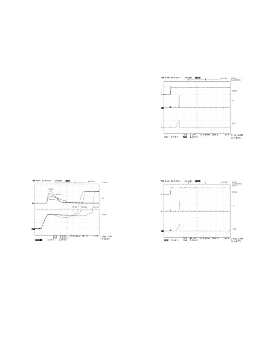
Turn On Clamp
Hotswap controllers using a MOSFET as the pass element all
include a capacitor divider from V
PP
to V
NN
through C
LOAD
, C
RSS
and C
GS
. In most competitive solutions a large external capacitor
is added to the gate of the pass element to limit the voltage on
the gate resulting from this divider. In those instances if a gate
capacitor is not used the internal circuitry is not available to hold
off the gate and therefore a fast rising voltage input will cause the
pass element to turn on for a moment. This allows current spikes
to pass through the MOSFET.
The HV100/HV101 include a built-in clamp to ensure that this
spurious current glitch does not occur. The built-in clamp will
work for the time constants of most mechanical connectors.
There may be applications, however, that have rise times that
are much less than 1
�
s (100's of ns). In these instances it may
be necessary to add a capacitor from the MOSFET gate to
source to clamp the gate and suppress this current spike. In
these cases the current spike generally contains very little
energy and does not cause damage even if a capacitor is not
used at the gate.
Auto-Adapt Operation
The HV100/HV101 Auto-adapt mechanism provides an impor-
tant function. It normalizes the hotswap period regardless of
pass element or load capacitor for consistent hotswap results.
By doing this it allows the novel short circuit mechanism to work
because the mechanism requires a known time base.
The above diagram illustrates the effectiveness of the auto-
adapt mechanism. In this example three MOSFETs with different
C
ISS
and R
DSON
values are used. The top waveform is the hotswap
current, while the bottom waveform is the gate voltage. As can
be seen, the hotswap period is normalized, the initial slope of the
gate voltage is approximately 2.5V/ms regardless of the MOSFET,
and the total hotswap period and peak currents are a function of
a MOSFET type dependent constant multiplied by C
LOAD
.
Typically if MOSFETs of the same type are used, the hotswap
results will be extremely consistent. If different types are used
they will usually exhibit minimal variation.
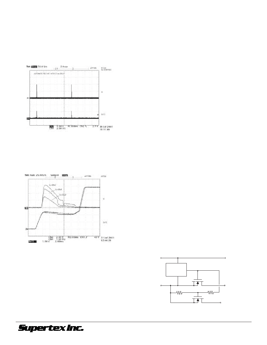
Short Circuit Protection
The HV100/HV101 provide short circuit protection by shutting
down if the Miller Effect associated with hotswap does not occur.
Specifically, if the output is shorted then the gate will rise without
exhibiting a "flat response". Due to the fact that we have normal-
ized the hotswap period for any pass element, a timer can be
used to detect if the gate voltage rises above a threshold within
that time, indicating that a short exists. The diagram below
shows a typical turn on sequence with the load shorted, resulting
in a peak current of 4A.
The maximum current that may occur during this period can be
controlled by adding a resistor in series with the source of the
MOSFET. The lower graph shows the same circuit with a 100m
resistor inserted between source and V
NN
. In this case the
maximum current is 25% smaller.
For most applications and pass elements, the HV100/HV101
provides adequate limiting of the maximum current to prevent
damage without the need for any external components. The 2.5s
delay of the auto-retry circuit provides time for the pass element
to cool between attempts.
2A/div
NTE66 is a trademark of NTE Electronics
IRF530 is a trademark of International Rectifier Corporation
IRF120M is a trademark of International Rectifier Corporation
5
HV100/HV101
1235 Bordeaux Drive, Sunnyvale, CA 94089
TEL: (408) 744-0100 � FAX: (408) 222-4895
www.supertex.com
08/26/02 rev.3b
�2002 Supertex Inc. All rights reserved. Unauthorized use or reproduction prohibited.
Application Information, cont'd.
Auto-Retry
Not only does the HV100/HV101 provide short circuit protection
in a 3-pin package, it also includes a 2.5s built in auto-restart
timer. The HV100/HV101 will continuously try to turn on the
system every 2.5s, providing sufficient time for the pass element
to cool down after each attempt.
Calculating Inrush Current
As can be seen in the diagram below, for a standard pass
element, the HV100/HV101 will normalize the hotswap time
period against load capacitance. For this reason the current limit
will increase with increasing value of the load capacitance.
Inrush can be calculated from the following formula:
I
INRUSH(PEAK)
= (C
ISS
/ C
RSS
) * 2.5e3 * C
LOAD
This is a surprisingly consistent result because for most MOSFETs
of a particular type the ratio of C
ISS
/ C
RSS
is relatively constant
(though notice from the plot that there is some variation) even
while the absolute value of these and other quantities vary.
Based on this, the inrush current will vary primarily with C
LOAD
.
This makes designing with the HV100/HV101 particularly easy
because once the pass element is chosen, the period is fixed and
the inrush varies with C
LOAD
only.
Programming the HV100/HV101
The HV100/HV101 require no external components other than a
pass element to provide the functionality described thus far. In
some applications it may be useful to use external components
to adjust the maximum allowable inrush current, adjust UVLO, or
to provide additional gate clamping if the supply rails have rise
times below 1ms.
All of the above are possible with a minimum number of external
components.
i)
To adjust inrush current with an external component simply
connect a capacitor (C
FB
) from drain to gate of the MOSFET.
The inrush calculation then becomes:
I
INRUSH
= (C
ISS
/ (C
RSS
+ C
FB
)) * 2.5e3 * C
LOAD
Note that a resistor (approximately 10K
) needs to be
added in series with C
FB
to create a zero in the feedback loop
and limit the spurious turn on which is now enhanced by the
larger divider element.
ii)
To increase undervoltage lockout simply connect a Zener
diode in series with the V
PP
pin.
iii)
If the V
PP
rises particularly fast (>48e6V/s) then it may be
desirable to connect a capacitor from gate to source of the
MOSFET to provide a path for the power application tran-
sient spike, which is now too fast for the internal clamping
mechanism.
iv)
To limit the peak current during a short circuit, a resistor in
series with the source of the MOSFET may help.
Implementing PWRGD Control
Due to the HV100/HV101's small footprint, it is possible to create
an open drain PWRGD signal using external components and
still maintain a size comparable with the smallest hotswap
controllers available elsewhere. To accomplish this an external
MOSFET may be used in conjunction with the gate output.
Simply use a high impedance divider (10M
) sized so that the
open drain PWRGD MOSFET threshold will only be reached
once the HV100/HV101's gate voltage rises well above the
current limit value required by the external MOSFET pass
device. Alternatively a Zener diode between the gate output and
the PWRGD MOSFET gate set at a voltage higher than the
maximum pass element Vt will also work.
2A/div
HV100
PWGRD