 | –≠–ª–µ–∫—Ç—Ä–æ–Ω–Ω—ã–π –∫–æ–º–ø–æ–Ω–µ–Ω—Ç: HV219FG | –°–∫–∞—á–∞—Ç—å:  PDF PDF  ZIP ZIP |
HV219
Rev. 2 110504
1
Low Charge Injection
8-Channel High Voltage Analog Switch
Features
!
HVCMOS technology for high performance
!
Very low quiescent power dissipation-10µA
!
Output On-resistance typically 11
!
Low parasitic capacitance
!
DC to 10MHz analog signal frequency
!
-60dB typical off-isolation at 5MHz
!
CMOS logic circuitry for low power
!
Excellent noise immunity
!
Serial shift register logic control with latches
!
Flexible operating supply voltages
!
Surface mount packages
Applications
!
Medical Ultrasound Imaging
!
Non-Destructive Evaluation
General Description
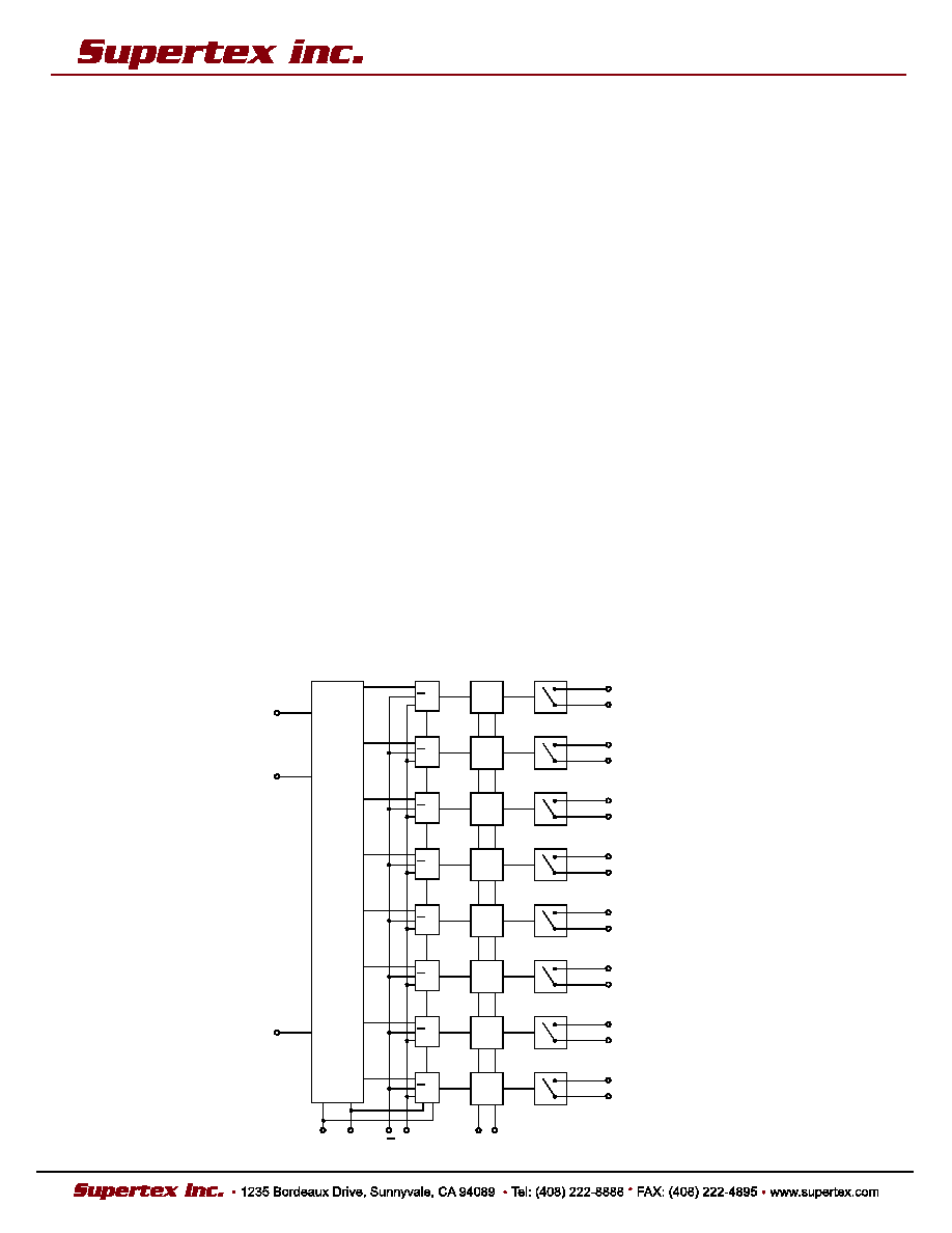
The Supertex HV219 is a low switch resistance, low charge
injection 8-channel 200V analog switch integrated circuit (IC)
intended primarily for medical ultrasound imaging. The device can
also be used for NDE, non-destructive evaluation applications. The
HV219 is a lower switch resistance, 11ohms versus 22ohms,
version of the Supertex HV20220 device. The lower switch
resistance will help reduce insertion loss. It has the same pin
configuration as that of the Supertex HV20220PJ and the
HV20220FG.
The device is manufactured using Supertex's HVCMOS (high
voltage CMOS) technology with high voltage bilateral DMOS
structures for the outputs and low voltage CMOS logic for the input
control. The outputs are configured as eight independent single
pole single throw 11 ohms analog switches. The input logic is an 8-
bit serial to parallel shift register followed by an 8-bit parallel latch.
The switch states are determined by the data in the latch. Logic
high will correspond to a closed switch and logic low as an opened
switch.
The HV219 is designed to operate on various combinations of high
voltage supplies. For example the V
PP
and V
NN
supplies can be:
+40V/-160V, +100V/-100V, or +160V/-40V. This allows the user to
maximize the signal voltage for uni-polar negative, bi-polar, or uni-
polar positive.
Block Diagram
HV219
Initial Release
A042705
SW0
D
LE
CL
LE
CL
D
LE
CL
D
LE
CL
D
LE
CL
D
LE
CL
D
LE
CL
D
LE
CL
D
LE
CL
8 BIT
SHIFT
REGISTER
LEVEL
SHIFTERS
OUTP UT
SWITCHES
LATCHES
V
PP
V
NN
V
DD
D
OUT
D
IN
CLK
SW1
SW2
SW3
SW4
SW5
SW6
SW7
GND
HV219
A042705
2
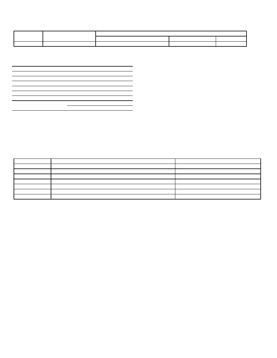
Ordering Information
Package Options
V
PP
-V
NN
Maximum Analog
Switch Voltage
28-lead plastic chip carrier PLCC
48-lead TQFP
Die
200V 180V
P-P
HV219PJ
HV219FG
HV219X
Absolute Maximum Ratings*
V
DD
Logic supply
-0.5V to +15V
V
PP
-V
NN
differential supply
220V
V
PP
Positive supply
-0.5V to V
NN
+200V
V
NN
Negative supply
+0.5V to ≠200V
Logic input voltage
-0.5V to V
DD
+0.3V
Analog signal range
V
NN
to V
PP
Peak analog signal current
3.0A
Storage temperature
-65∞C to +125∞C
28-Lead PLCC
1.2W
Power dissipation
48 Lead TQFP
1.0W
*Absolute Maximum Ratings are those values beyond which damage to the
device may occur. Functional operation under these conditions is not
implied. Continuous operation of the device at the absolute rating level may
affect device reliability. All voltages are referenced to device ground.
Operating Conditions
Symbol Parameter
Value
V
DD
Logic power supply
4.5V to 13.2V
V
PP
Positive high voltage supply
40V to V
NN
+200V
V
NN
Negative high voltage supply
-40V to -160V
V
IH
Input logic voltage high
V
DD
-1.5V to V
DD
V
IL
Input logic voltage low
0V to 1.5V
V
SIG
Analog signal voltage peak to peak
V
NN
+10V to V
PP
-10V
T
A
Operating free air temperature
0∞C to 70∞C
HV219
A042705
3
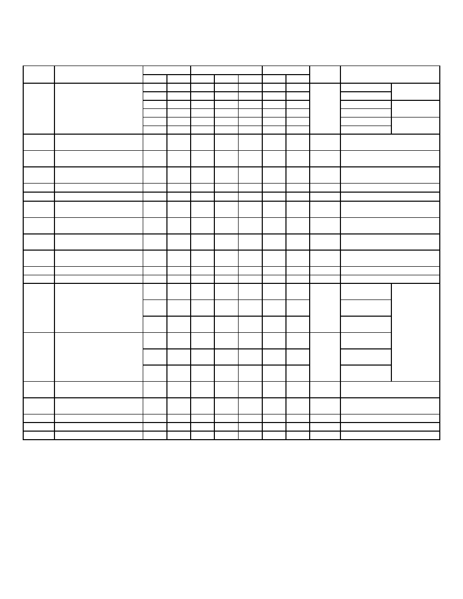
Electrical Characteristics
DC Characteristics
(over recommended operating conditions unless otherwise noted)
0∞C +25∞C
+70∞C
Sym Parameter
Min Max Min Typ Max Min Max
Units Conditions
15 13 19 24
I
SIG
= 5mA
13 11 14 16
I
SIG
= 200mA
V
PP
= +40V
V
NN
= -160V
13 11 14 15
I
SIG
= 5mA
9 9
12 14
I
SIG
= 200mA
V
PP
= +100V
V
NN
= -100V
12 10 13 15
I
SIG
= 5mA
R
ONS
Small Signal Switch
On-Resistance
11 8 13 14
Ohms
I
SIG
= 200mA
V
PP
= +160V
V
NN
= -40V
R
ONS
Small Signal Switch
On-Resistance Matching
20 5.0
20 20 %
I
SIG
= 5mA, V
PP
= +100V,
V
NN
= -100V
R
ONL
Large Signal Switch
On-Resistance
8
Ohms
V
SIG
= V
PP
-10V, I
SIG
= 1A
I
SOL
Switch Off Leakage per
Switch
5.0 1.0 10 15 µA
V
SIG
= V
PP
-10V and V
NN
+10V
DC offset Switch off
300
100
300
300
mV
R
LOAD
= 100K
DC offset Switch on
500
100
500
500
mV
R
LOAD
= 100K
I
PPQ
Quiescent V
PP
supply
current
10
50 µA
All
switches
off
I
NNQ
Quiescent V
NN
supply
current
-10
-50
µA
All
switches
off
I
PPQ
Quiescent V
PP
supply
current
10
50 µA
All
switches
on,
I
SW
= 5mA
I
NNQ
Quiescent V
NN
supply
current
-10
-50
µA
All
switches
on,
I
SW
= 5mA
Switch output peak current
3.0 3.0
2.0 2.0 A V
SIG
duty cycle < 0.1%
f
SW
Output switch frequency
50
kHz
Duty cycle = 50%
6.5 7.0 8.0
V
PP
= +40V
V
NN
= -160V
4.0 5.0 5.5
V
PP
= +100V
V
NN
= -100V
I
PP
Average V
PP
supply
current
4.0 5.0 5.5
mA
V
PP
= +160V
V
NN
= -40V
6.5 7.0 8.0
V
PP
= +40V
V
NN
= -160V
4.0 5.0 5.5
V
PP
= +100V
V
NN
= -100V
I
NN
Average V
NN
supply
current
4.0 5.0 5.5
mA
V
PP
= +160V
V
NN
= -40V
All output
switches are
turning On
and Off at
50KHz with
no load.
I
DD
Average V
DD
supply
current
4.0 4.0 4.0 mA
f
CLK
= 5MHz, V
DD
= 5.0V
I
DDQ
Quiescent V
DD
supply
current
10 10 10 µA
All
logic
inputs
are
static
I
SOR
Data out source current
0.45 0.45
0.70 0.40 mA V
OUT
= V
DD
-0.7V
I
SINK
Data out sink current
0.45 0.45
0.70 0.40 mA V
OUT
= 0.7V
C
IN
Logic
input
capacitance 10 10 10 pF
HV219
A042705
4
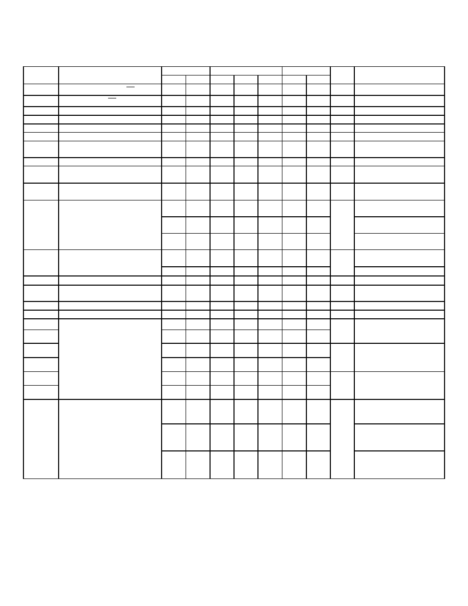
Electrical Characteristics
AC Characteristics
(over recommended operating conditions, V
DD
=5.0V, unless otherwise noted)
0∞C +25∞C
+70∞C
Sym Parameter
Min Max Min Typ Max Min Max
Unit
s
Conditions
t
SD
Set Up Time Before LE Rises
150 150 150 ns
t
WLE
Time Width of LE
150 150 150 ns
t
DO
Clock Delay Time to Data out
150
150
150
ns
tw
CL
Time Width of CL
150
150
150
ns
t
SU
Set Up Time Data to Clock
15
15
8.0
20
ns
t
H
Hold
Time
Data
from
Clock 35 35 35 ns
f
CLK
Clock
Frequency
5.0 5.0 5.0
MHz
50% duty cycle,
f
DATA
= f
CLK
/2
tr,tf Clock
rise
and
fall
Times
50 50 50 ns
Ton Turn
on
Time
5.0 5.0 5.0 µs
V
SIG
= V
PP
-10V,
R
LOAD
= 10K
Toff Turn
off
Time
5.0 5.0 5.0 µs
V
SIG
= V
PP
-10V,
R
LOAD
= 10K
20 20 20
V
PP
= +40V,
V
NN
= -160V
20 20 20
V
PP
= +100V,
V
NN
= -100V
dv/dt Maximum
V
SIG
Slew Rate
20 20 20
V/ns
V
PP
= +160V,
V
NN
= -40V
-30 -30
-33 -30
F = 5MHz, 1K
//15pF
load
KO Off
Isolation
-58 -58 -58
dB
F = 5.0MHz, 50
load
Kcr
Switch
Crosstalk
-60
dB
F = 5.0MHz, 50
load
Iid
Output Switch Isolation Diode
Current
300 300 300
mA
300ns pulse width, 2.0%
duty cycle
C
SG
(off)
Off Capacitance SW to Gnd
14
25
14
20
25
14
25
pF
0V, f = 1MHz
C
SG
(on)
On Capacitance SW to Gnd
40
60
40
50
60
40
60
pF
0V, f = 1MHz
+V
SPK
150
-V
SPK
200
mV
V
PP
= +40V,
V
NN
= -160V,
R
LOAD
= 50ohm
+V
SPK
150
-V
SPK
200
mV
V
PP
= +100V,
V
NN
= -100V,
R
LOAD
= 50ohm
+V
SPK
150
-V
SPK
Output Voltage Spike
200
mV
V
PP
= +160V,
V
NN
= -40V,
R
LOAD
= 50ohm
1450
V
PP
= +40V,
V
NN
= -160V,
V
SIG
= 0V
1050
V
PP
= +100V,
V
NN
= -100V,
V
SIG
= 0V
Q Charge
Injection
550
pC
V
PP
= +160V,
V
NN
= -40V,
V
SIG
= 0V
HV219
A042705
5
Power Up/Down Sequence
1)
Power up/down sequence is arbitrary except GND must be powered up first and powered down last. This applies for
applications powering GND of the IC with different voltages.
2)
Vsig must always be at or in between V
PP
and V
NN
or floating during power up/down transition.
3)
Rise and fall times of the power supplies V
DD
, V
PP
, and V
NN
should not be less than 1.0ms.
Logic Truth Table
Data in the 8-bit Shift Register
Output Switch State
D0 D1 D2 D3 D4 D5 D6 D7
LE CL
SW0 SW1 SW2 SW3 SW4 SW5 SW6 SW7
L
L
L
OFF
H
L
L
ON
L
L
L
OFF
H
L
L
ON
L L L
OFF
H L L
ON
L L L
OFF
H L L
ON
L
L
L
OFF
H
L
L
ON
L
L
L
OFF
H
L
L
ON
L L L
OFF
H L L
ON
L
L
L
OFF
H
L
L
ON
X X X X X X X X H L
HOLD
PREVIOUS
STATE
X X X X X X X X X H OFF OFF
OFF
OFF
OFF
OFF
OFF
OFF
Notes:
1.
The eight switches operate independently.
2.
Serial data is clocked in on the L to H transition clock.
3.
The switches go to a state retaining their present condition at the rising edge of the
LE
.
4. When
LE
is low, the shift register data flows through the latch.
5.
Shift register clocking has no effect on the switch states if
LE
is high.
6.
The clear input overrides all other inputs.
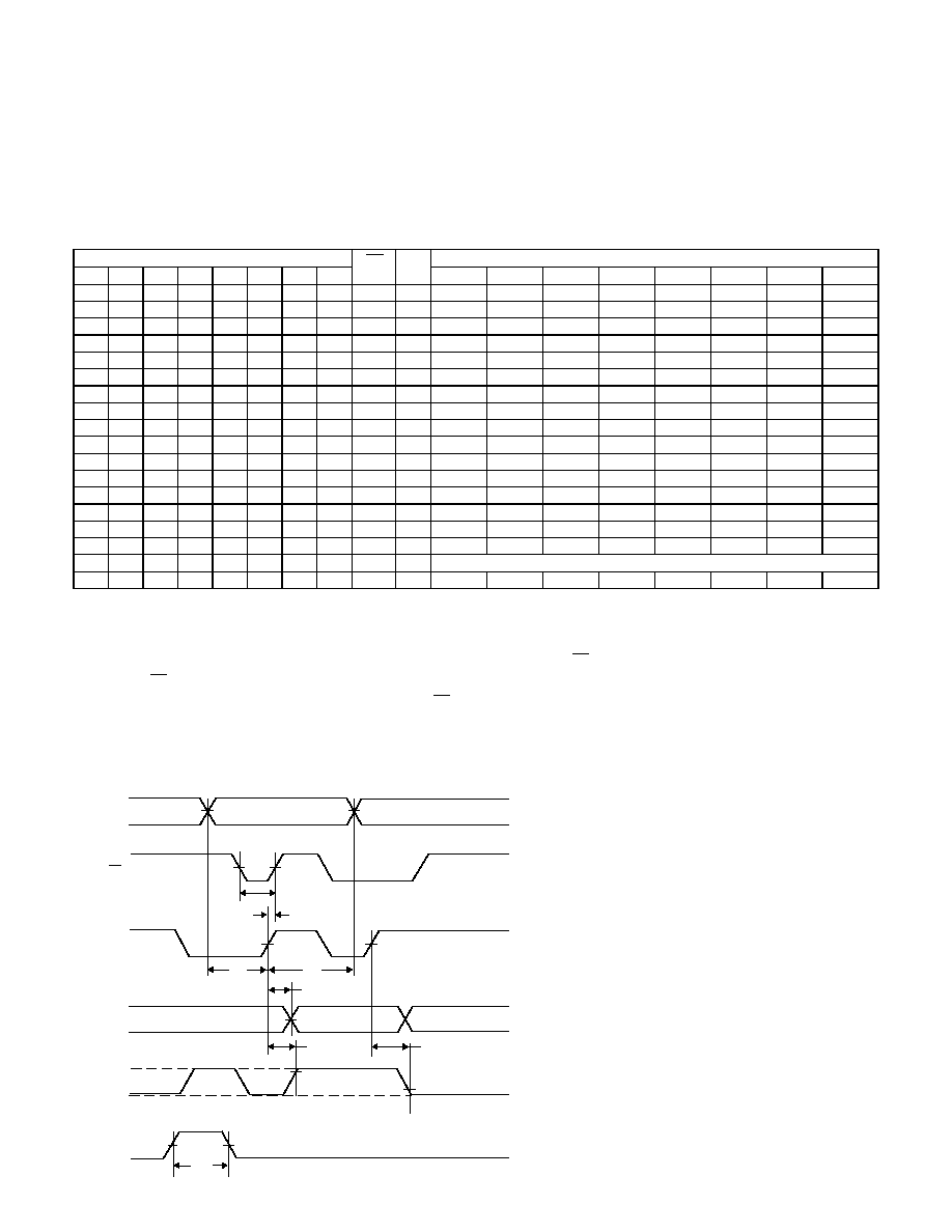
Logic Timing Waveform
DATA
IN
LE
CLOCK
DATA
OUT
D
N - 1
N
N + 1
D
D
50%
50%
50%
50%
50%
50%
50%
50%
50%
OUT
(TYP)
V OFF
ON
CLR
t
WCL
90%
10%
t
OFF
DD
SD
ON
t
t
t
t
t
h
WLE
SU
t