 | –≠–ª–µ–∫—Ç—Ä–æ–Ω–Ω—ã–π –∫–æ–º–ø–æ–Ω–µ–Ω—Ç: HV238 | –°–∫–∞—á–∞—Ç—å:  PDF PDF  ZIP ZIP |
1
16 Channel High Voltage Analog Switch
With Bleed Resistors
Features
!
HVCMOS technology for high performance
!
220V operating conditions
!
Output On-resistance typically 22
!
Integrated bleed resistors on the outputs
!
5.0V and 12.0V CMOS logic compatibility
!
Very low quiescent power dissipation -10µA
!
-45dB min off isolation at 7.5MHz
!
Low parasitic capacitance
!
Excellent noise immunity
!
Flexible operating supply voltages
Applications
!
Medical ultrasound imaging
!
Non-destructive evaluation
Description
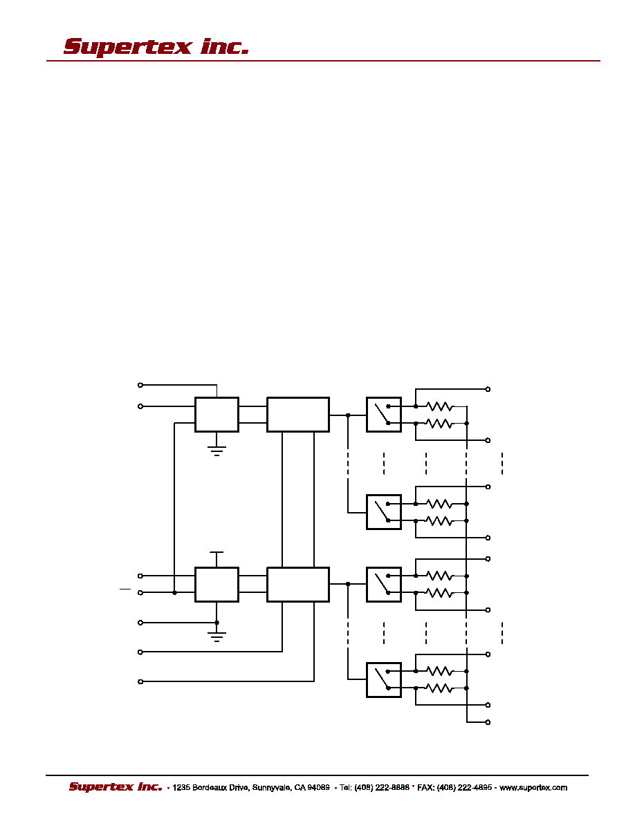
The Supertex HV238 is a 220V 16-channel high voltage
analog switch integrated circuit (IC) with output bleed
resistors (R
INT
). The output switches are configured as 2
sets of 8 single pole single throw analog switches. It is
intended to be used in applications requiring high voltage
switching controlled by low voltage control signals such as
ultrasound imaging.
The 2 sets of 8 analog switches are controlled by 2 input
logic controls, D
IN
1 and D
IN
2. A logic high on D
IN
1 will turn
ON switches 0 to 7 and a logic high on D
IN
2 will turn ON
switches 8 to 15. The bleed resistors help to significantly
reduce voltage built up on capacitive loads such as
piezoelectric transducers connected to the outputs.
Initial Release
HV238
Block Diagram
NR070805
LE
Latch
1
V
PP
V
NN
V
DD
D
IN
1
SW0
GND
Level
Translator 1
V
DD
SW0
SW7
SW7
SW8
SW8
SW15
SW15
Latch
2
Level
Translator 2
D
IN
2
R
GND
HV238
2
NR070805
Absolute Maximum Ratings*
V
DD
Logic supply
-0.5V to +15V
V
PP
-V
NN
differential supply
225V
V
PP
Positive supply
-0.5V to V
NN
+225V
V
NN
Negative supply
+0.5V to ≠225V
Logic input voltage
-0.5V to V
DD
+0.3V
Analog signal range
V
NN
to V
PP
Peak analog signal current/channel
3.0A
Storage temperature
-65∞C to 150∞C
Power dissipation
48-lead TQFP
1.0W
*Absolute Maximum Ratings are those values beyond which damage to the device
may occur. Functional operation under these conditions is not implied. Continuous
operation of the device at the absolute rating level may affect device reliability.
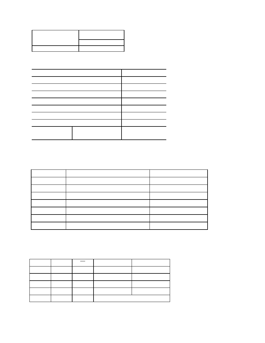
Ordering Information
Package Options
Device
48-lead TQFP
HV238 HV238FG
Operating Conditions*
Symbol Parameter
Value
V
PP
Positive high voltage supply
50V to 110V
V
NN
Negative high voltage supply
-10V to V
PP
≠220V
V
DD
Logic power supply voltage
4.75V to 12.6V
V
IH
High level input voltage
V
DD
-1.0V to V
DD
V
IL
Low level input voltage
0V to 1.0V
V
SIG
Analog signal voltage peak-to-peak
V
NN
+10V to V
PP
-10V
T
A
Operating free air temperature
0∞C to 70∞C
* Notes:
1 Power up/down sequence is arbitrary except GND must be powered-up first and powered-down last.
2 V
SIG
must be within V
NN
and V
PP
or floating during power up/down transition.
3 Rise and fall times of power supplies V
DD
, V
PP
, and V
NN
should not be less than 1.0msec.
Truth Table
D
IN
2 D
IN
1
LE
SW0 to SW7
SW8 to SW15
L L L
OFF
OFF
L H L
ON
OFF
H L L
OFF
ON
H H L
ON
ON
X
X
H
Hold Previous State

HV238
3
NR070805
Electrical Characteristics
DC Characteristics
(over recommended operating conditions unless otherwise noted)
0∞C +25∞C
+70∞C
Sym
Parameter
Min Max Min Typ Max Min Max
Units Conditions
30 26 32 40
V
SIG
= 0V, I
SIG
= 5mA,
V
PP
= 50V, V
NN
= -170V
25 22 27 35
V
SIG
= 0V, I
SIG
= 200mA,
V
PP
= 50V, V
NN
= -170V
15 22 27 30
V
SIG
= 0V, I
SIG
= 5mA,
V
PP
= 110V, V
NN
= -110V
R
ONS
Small Signal Switch
On-Resistance
20 18 22 25
V
SIG
= 0V, I
SIG
= 200mA,
V
PP
= 110V, V
NN
= -110V
R
ONS
Small Signal Switch
On-Resistance
Matching
20 5.0
20 20 %
V
SIG
= 0V, I
SIG
= 5mA,
V
PP
= 110V, V
NN
= -110V
R
ONL
Large Signal
Switch
On-Resistance
15
V
SIG
= 0V, I
SIG
= 1.0A
R
INT
Output Switch
Shunt Resistance
20 35 50 K
Output Switch to R
GND
I
RINT
= 0.5mA
I
SOL
Switch Off Leakage
per Switch
5.0 1.0 10 15 µA
V
SIG
= V
PP
-10V and
V
NN
= +10V
DC offset
Switch off
300 100
300 300 mV No
Load
DC offset
Switch on
500 100
500 500 mV No
Load
I
PPQ
Quiescent V
PP
supply current
10
50 µA
All
switches
off
I
NNQ
Quiescent V
NN
supply current
-10
-50
µA
All
switches
off
I
PPQ
Quiescent V
PP
supply current
10
50 µA
All
switches
on,
I
SW
= 5mA
I
NNQ
Quiescent V
NN
supply current
-10
-50
µA
All
switches
on,
I
SW
= 5mA
Switch output peak
current
3.0 3.0
2.0 2.0 A V
SIG
duty cycle < 0.1%
f
SW
Output switch
frequency
50 kHz
Duty
cycle=50%
I
PP
Average V
PP
supply
current
6.5 8.8 10
I
NN
Average V
NN
supply current
8.1 -8.8 -10
mA
V
PP
= 50V, V
NN
= -170V, All
Switches turning ON and
OFF at 50kHz
I
PP
Average V
PP
supply
current
-8.1 6.3 6.9
I
NN
Average V
NN
supply current
5.0 -6.3 -6.9
mA
V
PP
= 110V, V
NN
= -110V, All
Switches turning ON and
OFF at 50kHz
I
DDQ
Quiescent V
DD
supply current
10 10 10 µA
All
logic
inputs
are
static
I
DD
Average V
DD
supply current
2.0 2.0 2.0 mA
D
IN
1 = D
IN
2 = 3MHz,
LE
= high
C
IN
Logic input
capacitance
10 10 10 pF

HV238
4
NR070805
Logic Timing Diagram
Electrical Characteristics
AC Characteristics
(over recommended operating conditions unless otherwise noted)
0∞C +25∞C
+70∞C
Sym Parameter
Min Max Min Typ Max Min Max
Units Conditions
t
WLE
Time Width of LE 150 150 150 ns
t
WDIN
Time Width of D
IN
150 150 150 ns
t
SD
Set Up Time
Before LE Rises
150 150 150 ns
T
ON
Turn
On
Time
2.0 2.0 2.0 µs
V
SIG
= V
PP
-10V,
R
LOAD
= 10K
T
OFF
Turn
Off
Time
2.0 2.0 2.0 µs
V
SIG
= V
PP
-10V,
R
LOAD
= 10K
dv/dt
Maximum V
SIG
Slew Rate
20 20 20
V/ns
-30 -30
-33 -30
F = 5MHz,
Load = 1K
//15pF
KO Off
Isolation
-45 -45
-50 -45
dB
F = 7.5MHz,
R
LOAD
= 50
K
CR
Switch
Crosstalk -45 -45 -45 dB
F = 5.0MHz,
R
LOAD
= 50
I
ID
Output Switch
Isolation Diode
Current
300 300 300 mA
300ns pulse width,
2.0% duty cycle
C
SG(OFF)
Off Capacitance
Switch to Gnd
5.0 17 5.0 12 17 5.0 17 pF V
SIG
= 0V, f = 1.0MHz
C
SG(ON)
On Capacitance
Swithc to Gnd
25 50 25 38 50 25 50 pF V
SIG
= 0V, f = 1.0MHz
+V
SPK
4.0
-V
SPK
Output Voltage
Spike
-4.0
V
R
LOAD
= 50
0V
V
DD
D
IN
t
sd
t
WLE
LE
SW
ON
OFF
10%
90%
50%
0V
V
DD
T
ON
T
OFF
50%
50%
50%
HV238
5
NR070805
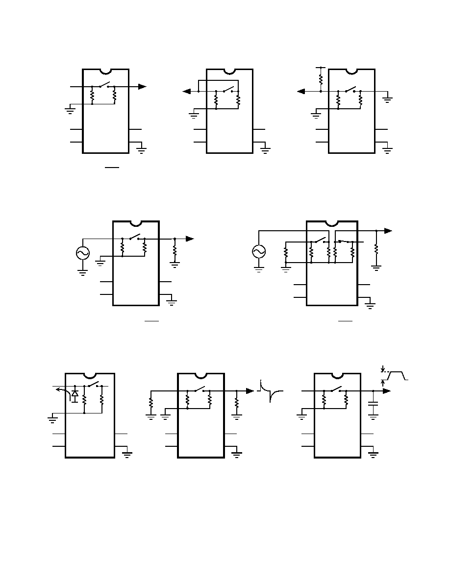
Test Circuits
V
PP
V
NN
V
DD
GND
5.0V
DC Offset ON/OFF
R
GND
V
OUT
V
PP
V
NN
V
DD
GND
5.0V
T
ON
/T
OFF
R
GND
V
OUT
V
PP
V
NN
V
PP
V
NN
R
INT
R
INT
R
INT
R
INT
V
PP
-10V
R
L
10K
V
PP
V
NN
V
DD
GND
5.0V
Switch OFF Leakage
R
GND
V
PP
-10V and
V
NN
+10V
V
PP
V
NN
R
INT
R
INT
V
OUT
V
OUT
I
SOL
R
INT
=
V
PP
V
NN
V
DD
GND
5.0V
Off Isolation
R
GND
V
PP
V
NN
R
INT
R
INT
V
OUT
V
OUT
V
IN
KO = 20Log
R
LOAD
V
IN
=10V
P-P
@ 5.0MHz
V
PP
V
NN
V
DD
GND
5.0V
Crosstalk
R
GND
V
PP
V
NN
R
INT
R
INT
V
OUT
V
OUT
V
IN
K
CR
= 20Log
V
IN
=10V
P-P
@ 5.0MHz
50
NC
50
V
PP
V
NN
V
DD
GND
5.0V
Isolation Diode Current
R
GND
V
SIG
V
PP
V
NN
R
INT
R
INT
V
NN
I
ID
V
PP
V
NN
V
DD
GND
5.0V
Output Voltage Spike
R
GND
V
PP
V
NN
R
INT
R
INT
V
OUT
1K
50
+V
SPK
-V
SPK
V
PP
V
NN
V
DD
GND
5.0V
Charge Injection
R
GND
V
PP
V
NN
R
INT
R
INT
V
OUT
Q = 1000pF x
V
OUT
V
SIG
1000pF
V
OUT