 | –≠–ª–µ–∫—Ç—Ä–æ–Ω–Ω—ã–π –∫–æ–º–ø–æ–Ω–µ–Ω—Ç: HV312 | –°–∫–∞—á–∞—Ç—å:  PDF PDF  ZIP ZIP |
1 Rev. D 04/17/02
Supertex, Inc. 1235 Bordeaux Drive, Sunnyvale, CA 94089 TEL: (408) 744-0100 Fax: (408) 222-4895 www.supertex.com
HV302
HV312
__________________________________________________________________________________________________________________
Initial Release
Sequencing Hotswap Controllers
(Negative Supply Rail)
Features
-10V to 90V or +10V to +90V Operation
Four PWRGD Flags with Programmable Delays
Integrated "normally-on" Gate Clamp eliminates components
UV/OV Lock Out & Power-On-Reset (POR) for Debouncing
Sense resistor programmed Circuit Breaker & Servo Limit
Programmable Circuit Breaker Delay
Inrush control using either: Servo or Feedback Capacitor
Feedback to RAMP pin saves gate protection components
100ms Start Up Timeout Protection for Output Overload
Programmable Inrush Current di/dt Control
Programmable Auto-Retry (tens of seconds if desired)
Auto-Retry or Latched Operation
Application solution for input voltage step (diode "ORing")
Enable through Open Drain interface to UV or OV
Low Power, 0.6mA Active Mode, 0.4mA Sleep Mode
Small SOIC-14 Package
Applications
-48V Telecom and Networking
-24V Cellular and Fixed Wireless Systems
-24V PBX Systems
Power Over LAN (IEEE802.3)
Distributed Power Systems
Power Supply Control
+48V Servers and SANs
Hotswap Control of Diode ORed Multiple Power Sources
Cooling Fan Systems
General Description
The HV302 and HV312 Hotswap Controllers perform current
limiting, circuit breaker protection, over and under voltage
detection power management functions during insertion of cards or
modules into live backplanes and connectors. They may be used
in systems where active control is implemented in the negative
lead of supplies ranging from -10V to -90V or +10V to +90V.
During initial power application the external pass device is held off
by a "normally-on" circuit that clamps its gate low. Thereafter
UV/OV and power-on-reset work together to suppress gate turn on
due to contact bounce. When stable connection has been
established for the duration of a programmed time delay, the
inrush current is controlled and limited to a programmed level
using one of two possible methods; servo mode or drain to ramp
feedback capacitor mode. When charging of the load capacitor
is completed, the open drain PWRGD-A flag is asserted. Open
drain PWRGD-B, PWRGD-C and PWRGD-D flags are asserted
sequentially after the expiration of their respective programmed
time delays. Thereafter it transitions to a low power sleep mode
and continues to monitor current and input voltage. If full charging
of the load capacitor is not achieved within 100ms or the circuit
breaker is tripped at any time, the external pass device is turned
off and all four PWRGD flags are reset to the inactive state.
Thereafter a programmable auto-retry timer will hold the pass
device off to allow it to cool before resetting and initiating auto-
retry. The auto-retry can be disabled using a single resistor if
desired.
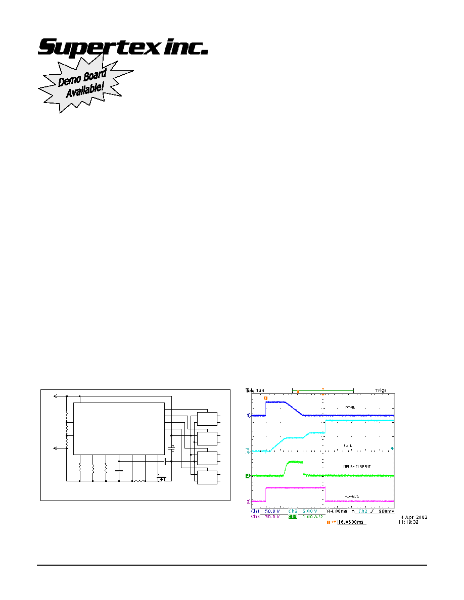
Typical Application Circuit and Waveforms
VDD
UV
OV
VEE
SENSE
GATE
RAMP
GND
-48V
IRF530
R4
R1
R2
R3
C1
Q1
HV302 / HV312
11
6
5
8
10
9
7
C2
1
Cload
+3.3V
DC/DC PWM
CONVERTER
COM
12
13
14
TB
TC
TD
2
3
4
+5V
DC/DC PWM
CONVERTER
COM
+12V
DC/DC PWM
CONVERTER
COM
-12V
DC/DC PWM
CONVERTER
COM
RTB
RTC
RTD
487k
6.81k
9.76k
0.0125
10nF
EN / EN
100uF
0.75nF
___
___
EN / EN
___
EN / EN
EN / EN
___
NOTES: 1. Under Voltage Shutdown (UV) set to 35V.
2. Over Voltage Shutdown (OV) set to 65V.
3. Current Limit set to -1A.
4. Circuit Breaker set to 8A.
PWRGD-A / PWRGD-A
________
PWRGD-B / PWRGD-B
________
PWRGD-C /PWRGD-C
________
PWRGD-D / PWRGD-D
________
2 Rev. D 04/17/02
HV302 / HV312
Absolute Maximum Ratings
Ordering Information
V
EE
reference to V
DD
pin
+0.3V to -100V
V
PWRGD
referenced to V
EE
Voltage
-0.3V to +100V
V
UV
and V
OV
referenced to V
EE
Voltage -0.3V to +12V
Operating Ambient Temperature
-40
∞
C to +85
∞
C
Operating Junction Temperature
-40
∞
C to +125
∞
C
Storage Temperature Range
-65
∞
C to +150
∞
C
Electrical Characteristics
(-10V VIN -90V, -40
∞
C
T
A
+85
∞
C unless otherwise noted)
Symbol Parameter Min
Typ
Max
Units
Conditions
Supply
(Referenced to V
DD
pin)
V
EE
Supply
Voltage
-90
-10
V
I
EE
Supply
Current
600
700
µ
A
V
EE
= -48V, Mode = Limiting
I
EE
Sleep Mode Supply Current
400
450
µ
A
V
EE
= -48V, Mode = Sleep
OV and UV Control
(Referenced to V
EE
pin)
V
UVH
UV High Threshold
1.26
V
Low to High Transition
V
UVL
UV Low Threshold
1.16
V
High to Low Transition
V
UVHY
UV
Hysteresis
100 mV
I
UV
UV Input Current
1.0
nA
V
UV
= V
EE
+ 1.9V
V
OVH
OV High Threshold
1.26
V
Low to High Transition
V
OVL
OV Low Threshold
1.16
V
High to Low Transition
V
OVHY
OV
Hysteresis
100 mV
I
OV
OV Input Current
1.0
nA
V
OV
= V
EE
+ 0.5V
Current Limit
(Referenced to V
EE
pin)
V
SENSE-CL
Current Limit Threshold Voltage
40
50
60
mV
V
UV
= V
EE
+ 1.9V, V
OV
= V
EE
+ 0.5V
V
SENSE-CB
Circuit Breaker Current Limit Threshold Voltage
80
100
120
mV
V
UV
= V
EE
+ 1.9V, V
OV
= V
EE
+ 0.5V
Gate Drive Output
(Referenced to V
EE
pin)
V
GATE
Maximum Gate Drive Voltage
8.5
10
12
V
V
UV
= V
EE
+ 1.9V, V
OV
= V
EE
+ 0.5V
I
GATEUP
Gate Drive Pull-Up Current
500
µ
A
V
UV
= V
EE
+ 1.9V, V
OV
= V
EE
+ 0.5V
I
GATEDOWN
Gate Drive Pull-Down Current
40
mA
V
UV
= V
EE
, V
OV
= V
EE
+ 0.5V
Ramp Timing Control
-
Test Conditions: C
LOAD
=100
µ
F, C
RAMP
=10nF, V
UV
= V
EE
+ 1.9V, V
OV
= V
EE
+ 0.5V, External MOSFET is IRF530*
I
RAMP
Ramp Pin Output Current
10
µ
A
V
SENSE
= 0V
t
POR
Time from UV to Gate Turn On
2.0
ms
(See Note 1)
t
RISE
Time from Gate Turn On to V
SENSE
Limit
400
µ
s
t
LIMIT
Duration of Current Limit Mode
5.0
ms
t
PWRGD-A
Time from Current Limit to PWRGD-A
5.0
ms
t
PWRGD-B
Maximum Time from PWRGD-A to PWRGD-B
150
200
250
ms
R
TB
= 120k
t
PWRGD-B
Minimum Time from PWRGD-A to PWRGD-B
3.0
5.0
8.0
ms
R
TB
= 3k
t
PWRGD-C
Maximum Time from PWRGD-B to PWRGD-C
150
200
250
ms
R
TC
= 120k
t
PWRGD-C
Minimum Time from PWRGD-B to PWRGD-C
3.0
5.0
8.0
ms
R
TC
= 3k
t
PWRGD-D
Maximum Time from PWRGD-C to PWRGD-D
150
200
250
ms
R
TD
= 120k
t
PWRGD-D
Minimum Time from PWRGD-C to PWRGD-D
3.0
5.0
8.0
ms
R
TD
= 3k
V
RAMP
Voltage on Ramp Pin in Current Limit Mode
3.6
V
(See Note 2)
t
STARTLIMIT
Start up Time Limit
80
100
120
ms
t
CBTRIP
Circuit Breaker Delay Time
2.0
5.0
µ
s
May be extended by external RC circuit
t
AUTO
Automatic Retry Delay
16
s
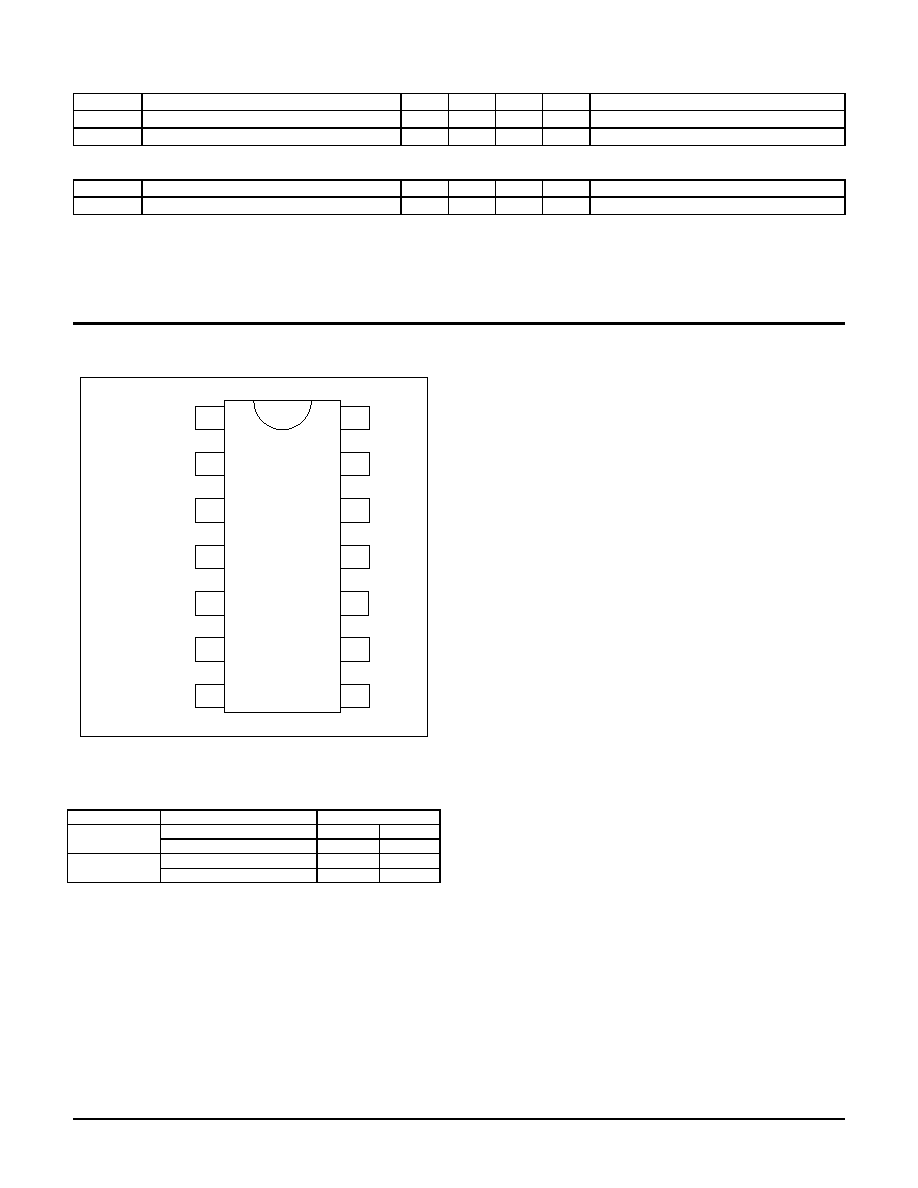
Package Options
Active State of Power
Good Flags
14 Pin SOIC
HIGH HV302NG
LOW HV312NG
Supertex, Inc. 1235 Bordeaux Drive, Sunnyvale, CA 94089 TEL: (408) 744-0100 Fax: (408) 222-4895 www.supertex.com
3 Rev. D 04/17/02
Power Good Outputs
(Referenced to V
EE
pin)
V
PWRGD-x(hi)
Power Good Pin Breakdown Voltage
90
V
PWRGD-x = HI Z
V
PWRGD-x(lo)
Power Good Pin Output Low Voltage
0.5
0.8
V
I
PWRGD
= 1mA, PWRGD-x = LOW
I
PWRGD-x(lk)
Maximum Leakage Current
<1.0
10
µ
A
V
PWRGD
= 90V, PWRGD-x = HI Z
Dynamic Characteristics
t
GATEHLOV
OV Comparator Transition
500
ns
t
GATEHLUV
UV Comparator Transition
500
ns
Note 1: This timing depends on the threshold voltage of the external N-Channel MOSFET. The higher its threshold is, the longer this timing.
Note 2: This voltage depends on the characteristics of the external N-Channel MOSFET. V
to
= 3V for an IRF530.
*IRF530 is a registered trademark of International Rectifier.
Pinout
4
5
6
7
8
9
10
11
1
2
3
12
13
14
PWRGD-D (HV312)
________
PWRGD-D (HV302)
PWRGD-C (HV312)
________
PWRGD-C (HV302)
PWRGD-B (HV312)
________
PWRGD-B (HV302)
PWRGD-A (HV312)
________
PWRGD-A (HV302)
OV
UV
VEE
VDD
TD
TC
TB
RAMP
GATE
SENSE
PWRGD Logic
Model Condition
PWRGD-A/B/C/D
INACTIVE (Not Ready)
0
V
EE
HV302
ACTIVE (Ready)
1
HI Z
INACTIVE (Not Ready)
1
HI Z
HV312
ACTIVE (Ready)
0
V
EE
Pin Description
PWRGD-D ≠ This Power Good Output Pin is held inactive on initial
power application and goes active a programmed time delay after
PWRGD-C goes active.
PWRGD-C ≠ This Power Good Output Pin is held inactive on initial
power application and goes active a programmed time delay after
PWRGD-B goes active.
PWRGD-B ≠ This Power Good Output Pin is held inactive on initial
power application and goes active a programmed time delay after
PWRGD-A goes active.
PWRGD-A ≠ This Power Good Output Pin is held inactive on initial
power application and goes active when the external MOSFET is
fully turned on.
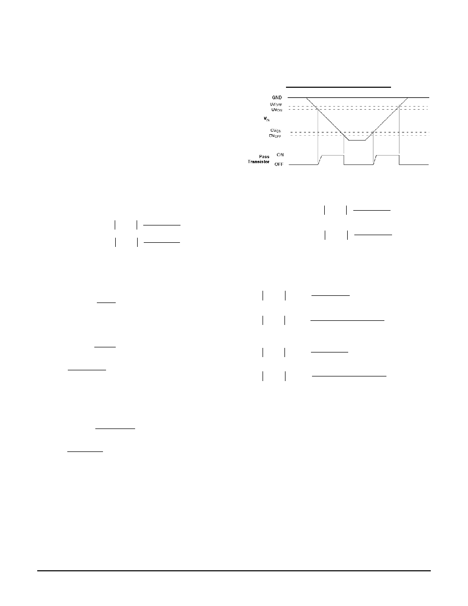
OV ≠ This Over Voltage (OV) sense pin, when raised above its
high threshold will immediately cause the GATE pin to be pulled
low. The GATE pin will remain low until the voltage on this pin falls
below the low threshold limit, initiating a new start-up cycle.
UV ≠ This Under Voltage (UV) sense pin, when below its low
threshold limit will immediately cause the GATE pin to be pulled
low. The GATE pin will remain low until the voltage on this pin
rises above the high threshold limit, initiating a new start-up cycle.
V
EE
≠ This pin is the negative terminal of the power supply input to
the circuit.
V
DD
≠ This pin is the positive terminal of the power supply input to
the circuit.
TD ≠ The resistor connected from this pin to V
EE
pin sets the time
delay from PWRGD-C going active to PWRGD-D going active.
TC ≠ The resistor connected from this pin to V
EE
pin sets the time
delay from PWRGD-B going active to PWRGD-C going active.
TB ≠ The resistor connected from this pin to V
EE
pin sets the time
delay from PWRGD-A going active to PWRGD-B going active.
RAMP ≠ This pin provides a current output so that a timing ramp
voltage is generated when a capacitor is connected.
GATE ≠ This is the Gate Driver Output for the external N-Channel
MOSFET.
SENSE ≠ The current sense resistor connected from this pin to V
EE
Pin programs the servo control current limit and the circuit breaker
trip limit.
Supertex, Inc. 1235 Bordeaux Drive, Sunnyvale, CA 94089 TEL: (408) 744-0100 Fax: (408) 222-4895 www.supertex.com

4 Rev. D 04/17/02
HV302 / HV312
Functional Block Diagram
LOGIC
C
Band Gap
Reference
Vbg
Internal
Supply
Regulator
Vint
C
UVLO
and
POR
gm
Transconductor
gm
2Vbg
Clamp Mechanism
Buffer
1 : 2
Mirror
10uA
Vint
C
Vint-1.2V
C
100mV
5k
5k
Transconductor
Circuit Breaker
Latch High & Sleep
TB TC TD
SENSE RAMP
GATE
555 type
Auto-Retry
Timer
Programmable
Timer
Selector
Switch
Selector
Switch
Vbg
UV
OV
VEE
PWRGD-A
PWRGD-B
PWRGD-C
PWRGD-D
VDD
Functional Description
Insertion into Hot Backplanes
Telecom, Networking, SAN and Server applications require the
ability to insert and remove circuit cards from systems without
powering down the entire system. All circuit cards have some filter
capacitance on the power rails, which is especially true in circuit
cards or network terminal equipment utilizing distributed power
systems. The insertion can result in high inrush currents that can
cause damage to connector and circuit cards and may result in
unacceptable disturbances on the system backplane power rails.
The HV302 and HV312 are designed to facilitate the insertion of
these circuit cards or connection of terminal equipment by
eliminating these inrush currents and powering up these circuits in
a controlled manner after full connector insertion has been
achieved
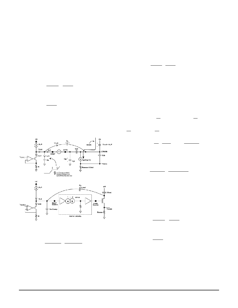
Description of Operation
During initial power application, a "normally-on" circuit holds off the
external MOSFET, preventing an input glitch while an integrated
regulator establishes an internal operating voltage of
approximately 10V. Until the proper internal voltage is achieved all
circuits are held reset, the PWRGD flags are inactive and the gate
to source voltage of the external MOSFET is clamped low.
Once the internal under voltage lock out (UVLO) has been
satisfied, the circuit checks the input supply under voltage (UV)
and over voltage (OV) sense circuits to ensure that the input
voltage is within programmed limits. These limits are determined
by the selected values of resistors R1, R2 and R3, which form a
voltage divider.
In Servo Mode operation, assuming the UV and OV limits are
satisfied and while continuing to hold the PWRGD flags inactive
and the external MOSFET GATE voltage low, the current source
feeding the RAMP pin is turned on. The external ramp capacitor
connected to it begins to charge, thus starting an initial time delay
determined by the value of the capacitor and the 2Vbg threshold
voltage of the RAMP pin. During this time if the OV or UV limits
are exceeded, an immediate reset occurs and the capacitor
connected to the RAMP pin is discharged.
When the voltage on the RAMP pin exceeds the 2Vbg threshold
voltage, the gate drive circuit begins to apply voltage to the gate of
the external MOSFET, which begins to turn on when its gate
threshold voltage is reached. The resulting output current
generates a voltage drop on the sense resistor connected between
the SENSE and V
EE
pins, causing a decrease in the available
current charging the capacitor on the RAMP pin. This continuous
feedback mechanism allows the output current to rise inverse
exponentially over a period of a few hundred microseconds to the
sense resistor programmed current limit set point.
When the voltage drop on the sense resistor reaches 50mV the
RAMP pin current is reduced to zero and the voltage on the RAMP
pin will be fixed, indicating that the circuit is in current limit mode.
Depending on the value of the load capacitor and the programmed
current limit, charging may continue for some time, but may not
exceed a nominal 100ms preset time limit. Once the load
capacitor has been charged, the output current will drop, reducing
the voltage on the SENSE pin, which in turn will increase the
RAMP pin current, thus causing the voltage on the capacitor
connected to the RAMP pin to continue rising, thereby providing
yet another programmed delay.
Supertex, Inc. 1235 Bordeaux Drive, Sunnyvale, CA 94089 TEL: (408) 744-0100 Fax: (408) 222-4895 www.supertex.com

5 Rev. D 04/17/02
HV302 / HV312
Functional Description -
continued
In Feedback Capacitor Mode operation, assuming the UV and
OV limits are satisfied and while continuing to hold the PWRGD
flags inactive and the external MOSFET GATE voltage low, the
current source feeding the RAMP pin is turned on. The external
ramp capacitor (C
RAMP
) begins to charge and the feedback
capacitor (C
FB
) begins to discharge, thus starting an initial time
delay determined by the equivalent value of the capacitors and the
2Vbg threshold voltage of the RAMP pin. During this time if the
OV or UV limits are exceeded, an immediate reset occurs, the
ramp capacitor is discharged and the feedback capacitor is
recharged.
When the voltage on the RAMP pin exceeds the 2Vbg threshold
voltage, the gate drive circuit begins to apply voltage to the gate of
the external MOSFET, which begins to turn on when its gate
threshold voltage is reached. However, the source current from
the RAMP pin limits the dv/dt of the feedback capacitor (C
FB
)
which, in turn, programs the inrush current limit (I
CL
) in accordance
with the relationship I
CL
= I
RAMP
x C
LOAD
/C
FB
and thus the dv/dt of the
load capacitor. At this point essentially all available current from
the RAMP pin flows into the feedback capacitor, thus the voltage
on the ramp capacitor and the RAMP pin remains essentially
constant, thereby limiting and controlling the gate voltage of the
external MOSFET (See Programming Current Limit and Circuit
Breaker in Design Information section). When the load capacitor is
fully charged the current flowing into the feedback capacitor is
reduced and the voltage drop across the MOSFET essentially
drops to zero, effectively connecting the feedback capacitor in
parallel with the ramp capacitor. Now the current from the RAMP
pin flows into the parallel-connected capacitors and the voltage on
the RAMP pin begins to rise, thereby providing yet another
programmed delay.
Whether operating in Servo Mode or Feedback Capacitor Mode,
when the ramp voltage is within 1.2V of the regulated internal
supply voltage, the controller will force the GATE terminal to a
nominal 10V, the PWRGD-A pin will change to an active state and
the Circuit Breaker is enabled. PWRGD-B will change to an active
state a programmed delay time after PWRGD-A went active,
PWRGD-C will change to an active state a programmed delay time
after PWRGD-B went active, PWRGD-D will change to an active
state a programmed delay time after PWRGD-C went active and
the circuit transitions to a low power sleep mode. While in sleep
mode the circuit continues to monitor the current and the OV and
UV status.
When the voltage on the SENSE pin rises to 100mV, indicating an
over current condition, the circuit breaker will trip in less than 5
µ
s.
This time may be extended by the addition of external
components.
If due to output overload conditions during startup full charging of
the load is not achieved within 100ms or a load fault occurs at any
time the circuit breaker is tripped, the MOSFET is turned off by
pulling down the GATE to V
EE
and all four PWRGD flags are reset.
Thereafter an auto-retry timer, programmed by the capacitor
connected to the RAMP pin, will hold the pass device off to allow it
to cool before resetting and restarting. The auto-retry can be
disabled using a single resistor if desired (See Auto-Retry and
Auto-Retry Disable in Design Information section).
At any time during the start up cycle or thereafter, crossing the UV
and OV limits (including hysteresis) will cause an immediate reset
of all internal circuitry. When the input supply voltage returns to a
value within the programmed UV and OV limits a new start up
sequence will be immediately initiated.
Supertex, Inc. 1235 Bordeaux Drive, Sunnyvale, CA 94089 TEL: (408) 744-0100 Fax: (408) 222-4895 www.supertex.com
6 Rev. D 04/17/02
HV302 / HV312
Design Information
Programming Under and Over Voltage Shut Down
The UV and OV pins are connected to comparators with nominal
1.21V thresholds and 100mV of hysteresis (1.21V
±
50mV). They
are used to detect under voltage and over voltage conditions at the
input to the circuit. Whenever the OV pin rises above its high
threshold (1.26V) or the UV pin falls below its low threshold
(1.16V) the GATE voltage is immediately pulled low, the PWRGD
pin changes to its inactive state and the external capacitor
connected to the RAMP pin is discharged.
Calculations can be based on either the desired input voltage
operating limits or the input voltage shutdown limits. In the
following equations the shutdown limits are assumed.
The under voltage and over voltage shut down thresholds can be
programmed by means of the three resistor divider formed by R1,
R2 and R3. Since the input currents on the UV and OV pins are
negligible the resistor values may be calculated as follows:
R3
R2
R1
R3
R2
V
1.16
V
UV
EEUV(off)
UVL
OFF
+
+
+
◊
=
=
=
R3
R2
R1
R3
V
1.26
V
OV
EEOV(off)
OVH
OFF
+
+
◊
=
=
=
Where
V
EEUV(off)
and
V
EEOV(off)
are Under & Over Voltage Shut
Down Threshold points.
If we select a divider current of 100
µ
A at a nominal operating input
voltage of 50 Volts then
500k
100uA
50V
R3
R2
R1
=
=
+
+
From the second equation for an OV shut down threshold of 65V
the value of R3 may be calculated.
500k
R3
65
1.26
OV
OFF
◊
=
=
9.69k
65
500K
1.26
R3
=
◊
=
The closest 1% value is 9.76k
From the first equation for a UV shut down threshold of 35V the
value of R2 can be calculated.
(
)
500K
R3
R2
35
1.16
UV
OFF
+
◊
=
=
6.81k
9.76k
35
500k
1.16
R2
=
-
◊
=
The closest 1% value is 6.81k
Then
483k
R3
R2
500K
R1
=
-
-
=
The closest 1% value is 487k
Under Voltage/Over Voltage Operation
From the calculated resistor values the OV and UV start up
threshold voltages can be calculated as follows:
R3
R2
R1
R3
R2
V
1.26
V
UV
EEUV(on)
UVH
ON
+
+
+
◊
=
=
=
R3
R2
R1
R3
V
1.16
V
OV
EEOV(on)
OVL
ON
+
+
◊
=
=
=
Where
V
EEUV(on)
and
V
EEOV(on)
are Under & Over Voltage Start
Up Threshold points.
Then
R3
R2
R3
R2
R1
1.26
V
EEUV(on)
+
+
+
◊
=
38.29V
9.76k
6.81k
9.76k
6.81k
487k
1.26
V
EEUV(on)
=
+
+
+
◊
=
And
R3
R3
R2
R1
1.16
V
EEOV(on)
+
+
◊
=
59.85V
9.76k
9.76k
6.81k
487k
1.16
V
EEOV(on)
=
+
+
◊
=
Therefore, the circuit will start when the input supply voltage is in
the range of 38.29V to 59.85V.
Supertex, Inc. 1235 Bordeaux Drive, Sunnyvale, CA 94089 TEL: (408) 744-0100 Fax: (408) 222-4895 www.supertex.com
7 Rev. D 04/17/02
HV302 / HV312
Design Information-
continued
Programming Current Limit and Circuit Breaker
Feedback Capacitor Mode Operation
In this operating mode the circuit breaker trip current and the
inrush current limit can be independently programmed. In fact the
circuit breaker can be completely disabled by setting R
SENSE
= 0
.
The circuit breaker will trip in less than 5
µ
s when the voltage on
the SENSE pin is raised 100mV above the V
EE
pin and the value of
the sense resistor may be calculated from the following equation:
CB
CB
CB
-
SENSE
SENSE
I
100mV
I
V
R
=
=
For an 8A circuit breaker:
12.5m
8A
100mV
R
SENSE
=
=
The power rating of the sense resistor must be greater than or
equal to I
CB
x V
SENSE-CB
.
The following diagrams depict the equivalent circuitry to clarify the
feedback capacitor operation for programming the inrush current
limit.
The inrush current limit may be programmed as follows:
Choose inrush current limit, for example I
CL
= 1A
Calculate
A
5
.
2
k
5
m
5
.
12
A
1
k
5
R
I
SENSE
CL
SINK
µ
=
◊
=
◊
=
I
If the Circuit Breaker function is disabled by setting R
SENSE
= 0
,
then I
SINK
= 0A. However, in this example we assume that the
Circuit Breaker function is enabled and therefore use I
SINK
= 2.5
µ
A.
Calculate C2 (feedback capacitor) discharge current
A
5
.
7
A
5
.
2
A
10
I
A
10
I
SINK
2
C
µ
=
µ
-
µ
=
-
µ
=
If Auto-Retry is disabled an adjustment must be made to I
C2
A
6
.
1
M
5
.
2
V
4
R
V
I
DISABLE
t
AUTO
µ
=
=
=
Where Vt is the maximum threshold voltage of the MOSFET.
Therefore, the adjusted value of I
C2
is:
AUTO
SINK
2
C
I
I
A
10
I
-
-
µ
=
A
9
.
5
A
6
.
1
A
5
.
2
A
10
I
2
C
µ
=
µ
-
µ
-
µ
=
In this example we assume that Auto-Retry is enabled and
therefore use I
C2
= 7.5
µ
A.
Note that
dt
dv
2
C
2
C
◊
=
I
and
dt
dv
C
LOAD
CL
◊
=
I
Since V
IN
is fixed and V
RAMP
is constant during limiting, then
dt
dv
across C
LOAD
=
dt
dv
across C2 as they share a common node
and their other terminals are at fixed voltages during inrush current
limiting. Therefore,
LOAD
CL
2
C
C
I
2
C
I
=
or
CL
LOAD
2
C
I
C
I
2
◊
=
C
.
As previously calculated and by conservation of charge on RAMP
node I
C2
=7.5
µ
A based on the chosen inrush current limit of I
CL
=1A.
Given that C
LOAD
=100
µ
F the required value for C2 can be
calculated.
Therefore
nF
75
.
0
A
1
F
100
A
5
.
7
I
C
I
2
CL
LOAD
2
C
=
µ
◊
µ
=
◊
=
C
Note that during initial power application the RAMP pin is voltage
protected by the capacitive AC voltage divider consisting of C
LOAD
,
C2 and C
RAMP
and the GATE pin is internally clamped.
Servo Control Mode Operation
The circuit breaker will trip in less than 5
µ
s when the voltage on
the SENSE pin is raised 100mV above the V
EE
pin and the value of
the sense resistor may be calculated from the following equation:
CB
CB
CB
-
SENSE
SENSE
I
100mV
I
V
R
=
=
For a 2A circuit breaker:
50m
2A
100mV
R
SENSE
=
=
The power rating of the sense resistor must be greater than or
equal to I
CB
x V
SENSE-CB
.
Supertex, Inc. 1235 Bordeaux Drive, Sunnyvale, CA 94089 TEL: (408) 744-0100 Fax: (408) 222-4895 www.supertex.com

8 Rev. D 04/17/02
HV302 / HV312
Design Information-
continued
The inrush current limit can be calculated as follows:
SENSE
SENSE
CL
-
SENSE
CL
R
50mV
R
V
I
=
=
Thus the inrush current limit for a 2A circuit breaker:
1A
50m
50mV
I
CL
=
=
Compensation components from gate to source of the external
MOSFET may be required to reduce peaking of the inrush current.
Compensation can be accomplished as follows:
1.
Start with a 2nF capacitor from gate to source.
2.
Increase capacitor value up to 10nF if needed.
3. If needed, add a 1k
resistor in series with the above
capacitor.
Servo Mode Timing
The timing functions are defined by the following equations:
RAMP
RAMP
START
I
C
4
.
2
t
=
RAMP
RAMP
)
th
(
GS
TH
I
C
V
t
=
TH
START
POR
t
t
t
+
=
-
FB
SENSE
LIMIT
RAMP
fs
RAMP
RISE
R
R
I
9
.
0
I
g
C
t
LIMIT
LOAD
IN
LIMIT
I
C
V
t
(
)
RAMP
RAMP
)
LIMIT
(
GS
INT
A
PWRGD
I
C
2
.
1
V
V
t
-
-
=
-
These equations assume that the load is purely capacitive and the
following definitions apply.
C
RAMP
is the external capacitor connected to the RAMP pin.
I
RAMP
is the output current from the RAMP pin, nominally
10
µ
A, when the voltage drop on R
SENSE
resistor is zero.
V
INT
is the internally regulated supply voltage and can range
from 9V to 11V.
V
GS(th)
is the gate threshold voltage of the external pass
transistor and may be obtained from its datasheet.
V
GS(limit)
is the external pass transistor gate-source voltage
required to obtain the limit current. It is dependent on the
pass transistor's characteristics and may be obtained from
the transfer characteristics on the transistor datasheet.
g
fs
is the transconductance of the external pass transistor and
may be obtained from its datasheet.
R
FB
is the internal feedback resistor and is nominally 5K
.
I
LIMIT
is the load current when the voltage drop on R
SENSE
resistor is 50mV.
These equations may be used to calculate the minimum value of
C
RAMP
for the most critical system performance characteristics.
For maximum contact bounce duration protection choose a value
for t
POR
and use the following equation:
)
it
(lim
GS
RAMP
POR
RAMP
V
4
.
2
I
t
C
+
◊
=
If control of PWRGD active delay is the critical system parameter,
then choose a value for t
PWRGD-A
and use the following equation:
2
.
1
V
V
I
t
C
)
it
(lim
GS
INT
RAMP
A
PWRGD
RAMP
-
-
◊
=
-
Supertex, Inc. 1235 Bordeaux Drive, Sunnyvale, CA 94089 TEL: (408) 744-0100 Fax: (408) 222-4895 www.supertex.com
9 Rev. D 04/17/02
HV302 / HV312
Design Information -
continued
Start up Overload Protection
Start up must be achieved within a nominal 100ms as indicated by
the PWRGD-A pin transition to the active state or the circuit will
reset and an Auto-Retry will initiate. If there is an output overload
or short circuit during start up, the circuit will be in current limit
mode for the 100ms time limit (in servo mode). In feedback
capacitor mode the circuit breaker will shutdown the MOSFET
before 100ms.
Circuit Breaker Delay
The circuit breaker will trip in less than 5
µ
s when the voltage on
the SENSE pin reaches a nominal 100mV. A resistor in series with
the SENSE pin and a capacitor connected between the SENSE
and VEE pins may be added to delay the rate of voltage rise on the
SENSE pin, thus permitting a current overshoot and delaying
Circuit Breaker activation. This method is particularly useful when
operating in Feedback Capacitor Mode. However, in Servo Mode
operation it will result in a current limit leading edge overshoot.
Auto-Retry and Auto-Retry Disable
The Auto-Retry delay time is directly proportional to the
capacitance at the RAMP pin. Auto-Retry sequence is activated
whenever the 100ms timeout is reached during start up or the
Circuit Breaker is tripped.
Auto-Retry can be approximated as a 555-timer with 2.5
µ
A charge
up and charge down currents through 8V, to a count of 256.
Therefore,
RAMP
try
Re
Auto
C
A
5
.
2
256
8
2
t
◊
µ
◊
◊
=
-
For C
RAMP
= 10nF
s
4
.
16
nF
10
A
5
.
2
256
8
2
t
try
Re
Auto
=
◊
µ
◊
◊
=
-
Due to the 2.5
µ
A maximum charge current a resistor which draws
more than 2.5
µ
A below 8V will disable Auto-Retry. Try to keep this
resistor as big as possible, e.g. 2.5M
. For most MOSFETs with
maximum Vt of 4V, this will vary the 10
µ
A RAMP current source by
only
A
6
.
1
M
5
.
2
V
4
µ
=
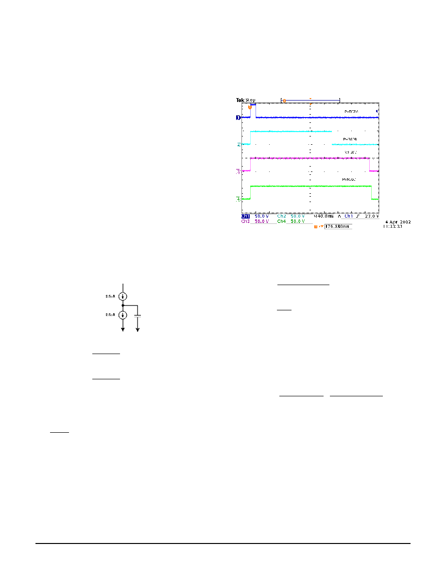
PWRGD Flag Delay Programming
Shortly after current limiting ends, PWRGD-A becomes active
indicating successful completion of the Hotswap operation.
PWRGD-B will change to an active state a programmed delay time
after PWRGD-A went active, PWRGD-C will change to an active
state a programmed delay time after PWRGD-B went active and
PWRGD-D will change to an active state a programmed delay time
after PWRGD-C went active. Resistors connected from the
respective TB, TC and TD pins to V
EE
pin are used to program the
delay times between the PWRGD flags sequentially going active.
The following waveforms demonstrate the sequencing of the
PWRGD flags. These results were obtained with R
TB
= 120k
, R
TC
= 60k
and R
TD
= 3k
The value of the resistors determines the capacitor charging and
discharging current of a triangle wave oscillator. The oscillator
output is fed to an 8-bit counter to generate the desired time delay.
The respective delay time is defined by the following equation:
CD
PP
OSC
TX
I
V
C
2
255
t
◊
◊
◊
=
and
TX
bg
CD
R
4
V
I
=
Where t
TX
= Delay Time between respective PWRGD flags
C
OSC
= 120pF (Internal oscillator capacitor)
V
PP
= 8.2V (Peak-to-Peak voltage swing of oscillator)
I
CD
= Charge and Discharge current of oscillator
Vbg = 1.2V (Internal Band Gap Reference)
R
TX
= Programming resistor at TB, TC or TD pin
Combining the above two equations and solving for R
TX
yields:
V
2
.
8
pF
120
2040
t
V
2
.
1
V
C
2040
t
B
R
TX
PP
PP
TX
bg
TX
◊
◊
◊
=
◊
◊
◊
=
TX
6
TX
t
10
6
.
0
R
◊
◊
=
For a delay time of 200ms we get:
(
) (
)
=
◊
◊
◊
=
-
k
120
10
200
10
6
.
0
R
3
6
TX
For a delay time of 5ms we get:
(
) (
)
=
◊
◊
◊
=
-
k
3
10
5
10
6
.
0
R
3
6
TX
Supertex, Inc. 1235 Bordeaux Drive, Sunnyvale, CA 94089 TEL: (408) 744-0100 Fax: (408) 222-4895 www.supertex.com

10 Rev. D 04/17/02
HV302 / HV312
Design Information -
continued
Supported External Pass Devices
The HV302 and HV312 are designed to support N-Channel
MOSFETs and IGBTs.
Selection of External Pass Devices
The R
DS(ON)
of the device is likely to be selected based on
allowable voltage drop at maximum load (I
LOAD(MAX)
) after the
Hotswap action has been completed. Thus the required
continuous power dissipation rating (P
CONT
) of the device can be
determined from the following equation:
)
MAX
(
LOAD
2
)
ON
(
DS
CONT
I
R
P
◊
=
The peak power rating (P
PEAK
) should be based on the highest
current level, which is always the circuit breaker trip set point (I
CB
),
and on the assumption that a output is shorted. The peak power
rating may be calculated from the following equation:
CB
IN
PEAK
I
V
P
◊
=
Given these values an external pass transistor may be selected
from the manufacturers data sheet.
Paralleling External Pass Transistors
Due to variations in threshold voltages and transconductance
characteristics between samples of MOSFETs, reliable 50%
current sharing is not achievable. Some measure of paralleling
may be accomplished by adding resistors in series with the source
of each device; however, it will cause increased voltage drop and
power dissipation.
Paralleling of external Pass devices is not recommended!
If a sufficiently high current rated external pass transistor cannot
be found then increased current capability may be achieved by
connecting independent Hotswap circuits in parallel, since they act
as current sources during the load capacitor charging time when
the circuits are in current limit. For this application the HV302 with
active high PWRGD is recommended where the PWRGD pins of
multiple Hotswap circuits can be connected in a wired OR
configuration.
Kelvin Connection to Sense Resistor
Physical layout of the printed circuit board is critical for correct
current sensing. Ideally trace routing between the current sense
resistor and the V
EE
and SENSE pins should be direct and as short
as possible with zero current in the sense traces. The use of
Kelvin connection from SENSE pin and V
EE
pin to the respective
ends of the current sense resistor is recommended.
To Negative
Terminal of
Power Source
To Source
of MOSFET
To
VEE
Pin
To
SENSE
Pin
Sense Resistor
Supertex, Inc. 1235 Bordeaux Drive, Sunnyvale, CA 94089 TEL: (408) 744-0100 Fax: (408) 222-4895 www.supertex.com