 | –≠–ª–µ–∫—Ç—Ä–æ–Ω–Ω—ã–π –∫–æ–º–ø–æ–Ω–µ–Ω—Ç: HV421 | –°–∫–∞—á–∞—Ç—å:  PDF PDF  ZIP ZIP |
11-1
11
Absolute Maximum Ratings*
Supply Voltage, V
DD
-0.5V to +10V
Output Voltage, V
cs
-0.5V to +120V
Operating Temperature Range
0∞C to +85∞C
Storage Temperature Range
-65∞C to +150∞C
SO-8 Power Dissipation
400mW
Note:
*All voltages are referenced to GND.
HV421
High Voltage 1 REN Ring Generator
Features
Processed with HVCMOS
Æ
technology
4.75V to 9.5V operating supply voltage
DC to AC conversion
1 REN load capacity
Adjustable ring frequency from 15Hz to 60Hz
Adjustable converter frequency
Enable/Disable function
Ordering Information
General Description
The Supertex HV421 is a high voltage ring generator designed
to drive 1 North American REN (ringer equivalent number) from
a 5V source. The HV421 has an internal DC-DC converter which
converts the 5V DC supply to a nominal 68V DC connected to the
V
PP
pin. The DC-DC converter frequency of the HV421 is set by
an external resistor connected between R
SW
and V
DD
. The
ringing signal is generated by a high voltage H-bridge which
produces two square waves which are 180 degrees from each
other. The ringing frequency of the H-bridge is set by an external
resistor connected between R
RING
and V
DD
.
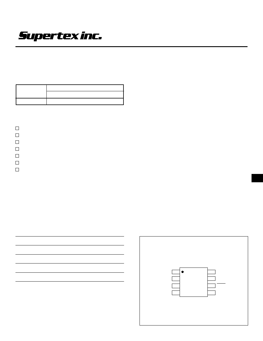
Pin Configuration
Package Options
Device
8-Lead SO
HV421
HV421LG
Top View
1
2
3
4
8
7
6
5
V
DD
R
ring
R
SW
Gate
V
PP
Gate
L
x
GND
SO-8
≠ OBSOLETE ≠

11-2
Symbol
Parameter
Min
Typ
Max
Units
Conditions
R
DS(ON)
On-resistance of switching transistor
3.5
5
I=100mA
I
DDQ
Quiescent V
DD
supply current
50
nA
R
SW
=Low
I
DD
Input current going into the V
DD
pin
300
µA
V
IN
=5.0V. See Figure 1.
I
IN
Input current including inductor current
170
220
mA
V
IN
=5.0V. See Figure 1.
V
PP
Output voltage on V
PP
65
68
V
V
IN
=5.0V. See Figure 1.
F
RING
Ring frequency
20
25
30
Hz
V
IN
=5.0V. See Figure 1.
D
RING
Ringing frequency duty cycle
50
%
fsw
Switching transistor frequency
35
KHz
V
IN
=5.0V. See Figure 1.
Dsw
Switching transistor duty cycle
88
%
Electrical Characteristics
DC Characteristics
(V
DD
=5.0V, R
RING
=30M, R
SW
=1.3M, L
X
=330µH, T
A
=25∞C)
Symbol
Parameter
Min
Typ
Max
Units
Conditions
V
DD
Supply voltage
4.75
9.5
V
T
A
Operating temperature
0
85
∞C
Recommended Operating Conditions
Symbol
Parameter
Min
Typ
Max
Units
Conditions
EN-L
Logic input low voltage
0
0.5
V
EN-H
Logic input high voltage
V
DD
-0.5
V
DD
V
Enable/Disable Table
HV421
≠ OBSOLETE ≠

11-3
11
Typical Application
Block Diagram
DC-DC
Converter
GND
V
DD
L
x
R
SW
R
RING
Level
Translator
Ring
Frequency
V
PP
Gate
Gate
30M
1.3M
0.01µF
V
IN
HV421LG
8
7
6
5
1
2
3
4
330µH
1N4148
V
DD
R
SW
V
PP
L
x
R
RING
Gate
Gate
GND
ON = 4.75V
OFF = 0V
Q1
Q2
Q3
8.0µF
Load
Q4
1.0µF
6.8K
4.75V
160mA
0.01µF
D1
D2
D3
D4
2.2K
2.2K
Q1, Q3 = Supertex VN2110K1
Q2, Q4 = Supertex VP2110K1
D1≠D4 = 5.1V Zener diode
V
OUT
= ±60V
Freq = 25Hz
Figure 1: 1 REN Ring Generator
HV421
≠ OBSOLETE ≠

11-4
Breakdown
Gate Threshold
Device
Type
Voltage, BV
DSS
Voltage, V
GS(th)
On-Resistance, R
DS(ON)
Package Options
VN2110
N-Channel
100V
0.8V to 2.4V
6.0 at V
GS
=5V
TO-92, SOT-23
VP2110
P-Channel
-100V
-1.5V to -3.5V
11 at V
GS
=-5V
TO-92, SOT-23
Application Description
The Supertex HV421LG is a high voltage 1 REN ring genera-
tor. A typical application circuit is shown in Figure 1. There are
four basic parts to the circuit; the DC-DC converter, level
translation of the ringing frequency, enable/disable function,
and an external source follower buffer stage.
Enable/Disable function
The HV421 can be enabled by connecting the 1.3M and
30M resistors to the same potential as V
DD
and disabled by
connecting them to ground.
DC-DC converter
The DC-DC converter consists of a 330µH inductor, 1N4148
diode, 1.0µF capacitor and 1.3M resistor. The 1.3M resistor
sets the DC-DC converter frequency. Energy is stored in the
330µH inductor when the switching transistor is turned on and
is released into the 1.0µF capacitor when the switch is in the
off state. A high voltage DC will develop at V
PP
which is
internally connected to the level translator.
Level translation of the ringing frequency
The ringing frequency is set by a 30M resistor. A low voltage
square wave is generated with a nominal frequency of 25Hz.
Lower ringing frequencies can be obtained by using resistors
greater than 30M. The signal is then level translated to swing
from 0V to the V
PP
voltage. An inverted and a noninverted
output are generated (gate and gate bar).
External source follower buffer stage
The gate and gate bar are connected to an external source
follower stage. Supertex transistors VP2110K1 and VN2110K1
are used for the buffering. Zener diodes clamps across the
gates are recommended as a precaution but not required.
The voltage seen by the load is ±60V. A 6.8K resistor in
series with an 8.0µF capacitor is used to simulate 1 North
American REN (ringer equivalent number). The main specifi-
cations for the Supertex source follower transistors are listed
below.
HV421
≠ OBSOLETE ≠

11-5
11
Absolute Maximum Ratings
V
PP1
- V
NN1
, power supply voltage
+340V
V
PP1
, positive high voltage supply
+220V
V
PP2
, positive gate voltage supply
+220V
V
NN1
, negative high voltage supply
-220V
V
NN2
, negative gate voltage supply
-220V
V
DD
, logic supply
+7.5V
Storage temperature
-65∞C to +150∞C
Power dissipation
800mW
Operating Voltage
Package Options
V
PP1
- V
NN1
SOW-20
325V
HV430WG
General Description
The Supertex HV430 is a high voltage PWM ring generator
integrated circuit. The high voltage outputs, Pgate and Ngate,
are used to drive the gates of external high voltage P-channel,
TP2640, and N-channel, TN2640, MOSFETs in a push-pull
configuration. Pulse by pulse over current protection are imple-
mented on both the P-channel and N-channel MOSFETs. The
RESET inputs functions as a power-on reset and as a low
voltage lockout, allowing for hot-swapping capabilities. The
FAULT output indicates over-current and low voltage lockout
conditions. It is active-low and open-drain to allow wire OR'ing of
multiple drivers.
P
GATE
and N
GATE
are controlled independently by logic inputs P
in
and N
in
when the mode pin is at logic high. A logic high on P
in
will
turn on the external P-channel MOSFET. Similarly, a logic high
on N
in
will turn on the external N-channel MOSFET. Lockout
circuitry prevents the N and P switches from turning on simulta-
neously.
For applications where a single control input is desired, the mode
pin should be connected to Gnd. The PWM control signal is then
input to the N
in
pin. A user-adjustable deadband in the control
logic assures break-before-make on the outputs, thus avoiding
cross conduction on the high voltage output during switching. A
logic high on Nin will turn the external P-Channel MOSFET on
and the N-Channel off, and vice versa. The IC can be powered
down by applying a logic low on the Enable pin, placing both
external MOSFETs in the off state.
Ordering Information
HV430
High-Voltage Ring Generator
Features
100V
RMS
ring signal
Output over current protection
5.0V CMOS logic control
Logic enable/disable to save power
Fault output for over-current and low voltage lockout
conditions
Adjustable deadband in single-control mode
Power-on reset for hot-swap protection
Low voltage lockout
Applications
High voltage ring generator
Set-top/Street box ring generator
Advanced Information