 | –≠–ª–µ–∫—Ç—Ä–æ–Ω–Ω—ã–π –∫–æ–º–ø–æ–Ω–µ–Ω—Ç: HV430 | –°–∫–∞—á–∞—Ç—å:  PDF PDF  ZIP ZIP |
1
HV430
High Voltage Ring Generator
Features
105Vrms ring signal
Output over current protection
5.0V CMOS logic control
Logic enable/disable to save power
Adjustable deadband in single-control mode
Power-on reset
Fault output for problem detection
Applications
Line access cards
Set-top/Street box
General Description
The Supertex HV430 is a high voltage PWM ring generator
integrated circuit. The high voltage outputs, V
PGATE
and V
NGATE
,
are used to drive the gates of external high voltage P-channel
and N-channel MOSFETs in a push-pull configuration. Over
current protection is implemented for both the P-channel and N-
channel MOSFETs. External sense resistors set the over-cur-
rent trip point.
The RESET input functions as a power-on reset when connected
to an external capacitor.
The FAULT output indicates an over-current condition and is
cleared after 4 consecutive cycles with no overcurrent condition.
A logic low on RESET or ENABLE clears the FAULT output. It is
active-low and open-drain to allow wire OR'ing of multiple
drivers.
P
gate
and N
gate
are controlled independently by logic inputs P
IN
and
N
IN
when the MODE pin is at logic high. A logic high on P
IN
will turn
on the external P-channel MOSFET. Similarly, a logic high on N
IN
will turn on the external N-channel MOSFET. Lockout circuitry
prevents the N and P switches from turning on simultaneously.
A pulse width limiter restricts pulse widths to no less than 100-
200ns.
For applications where a single control input is desired, the
MODE pin should be connected to SGND. The PWM control
signal is then input to the N
IN
pin. A user-adjustable deadband in
the control logic ensures break-before-make on the outputs,
thus avoiding cross conduction on the high voltage output during
switching. A logic high on N
IN
will turn the external P-Channel
MOSFET on and the N-Channel off, and vice versa. The IC can
be powered down by applying a logic low on the ENABLE pin,
placing both external MOSFETs in the off state.
Absolute Maximum Ratings
V
PP1
≠ V
NN1
, power supply voltage
+340V
V
PP1
, positive high voltage supply
+220V
V
PP2
, positive gate voltage supply
+220V
V
NN1
, negative high voltage supply
-220V
V
NN2
, negative gate voltage supply
-220V
V
DD
, logic supply
+7.5V
Storage temperature
-65∞C to +150∞C
Power dissipation
600mW
Ordering Information
Operating Voltage
Package Options
V
PP1
-V
NN1
SOW-20
325V
HV430WG
12/13/01
Supertex Inc. does not recommend the use of its products in life support applications and will not knowingly sell its products for use in such applications unless it receives an adequate "products liability
indemnification insurance agreement." Supertex does not assume responsibility for use of devices described and limits its liability to the replacement of devices determined to be defective due to
workmanship. No responsibility is assumed for possible omissions or inaccuracies. Circuitry and specifications are subject to change without notice. For the latest product specifications, refer to the
Supertex website: http://www.supertex.com. For complete liability information on all Supertex products, refer to the most current databook or to the Legal/Disclaimer page on the Supertex website.

2
Electrical Characteristics
(Over operating supply voltage unless otherwise specified, T
A
= -40∞C to +85∞C.)
External Supplies
Symbol
Parameter
Min
Typ
Max
Unit
Conditions
V
PP1
High voltage positive supply
50
200
V
I
PP1Q
V
PP
quiescent current
250
500
µA
P
IN
=N
IN
=0V
I
PP1
V
PP
operating current
2.0
mA
No load
V
OUTP
and V
OUTN
switching at 100kHz
V
NN1
High voltage negative supply
V
PP1
-325
-50
V
I
NN1Q
V
NN1
quiescent current
250
500
µA
P
IN
=N
IN
=0V, R
DB
=18k
I
NN1
V
NN1
operating current
1.0
mA
No load
V
OUTP
and V
OUTN
switching at 100kHz
V
DD
Logic supply voltage
4.50
5.50
V
I
DDQ
V
DD
quiescent current
300
400
µA
P
IN
=N
IN
=0V, R
DB
=18k
I
DD
V
DD
operating current
1.0
mA
P
IN
=N
IN
=100kHz, R
DB
=18k
Internal Supplies
Symbol
Parameter
Min
Typ
Max
Unit
Conditions
V
PP2
Positive linear regulator output voltage
V
PP1
-16
V
PP1
-10
V
V
NN2
Negative linear regulator output voltage
V
NN1
+10
V
NN1
+14
V
Positive High Voltage Output
Symbol
Parameter
Min
Typ
Max
Unit
Conditions
V
Pgate
Output voltage swing
V
PP2
V
PP1
V
No load on V
Pgate
R
sourceP
V
Pgate
source resistance
12.5
I
OUT
=80mA
R
sinkP
V
Pgate
sink resistance
12.5
I
OUT
=-80mA
t
riseP
V
Pgate
rise time
50
ns
C
load
=1.4nF
t
fallP
V
Pgate
fall time
50
ns
C
load
=1.4nF
t
pwp(min)
V
Pgate
minimum pulse width
(internally limited)
100
150
200
ns
t
delayP
P
IN
to Pgate delay time
300
ns
mode=1
V
Psen
V
Pgate
current sense voltage
V
PP1
-0.85
V
PP1
-1.0
V
PP1
-1.15
V
t
shortP
V
Pgate
current sense off time
150
ns
HV430
3
Negative High Voltage Output
Symbol
Parameter
Min
Typ
Max
Unit
Conditions
V
Ngate
Output voltage swing
V
NN2
V
NN1
V
No load on V
Ngate
R
sourceN
V
Ngate
source resistance
15.0
I
OUT
=80mA
R
sinkN
V
Ngate
sink resistance
15.0
I
OUT
=-80mA
t
riseN
V
Ngate
rise time
50
ns
C
load
=1.0nF
t
fallN
V
Ngate
fall time
50
ns
C
load
=1.0nF
t
pwn(min)
V
Ngate
minimum pulse width
(internally limited)
100
150
200
ns
t
delayN
N
IN
to V
Ngate
delay time
300
ns
mode=1
V
Nsen
V
Ngate
current sense voltage
V
NN1
+0.85
V
NN1
+1.0
V
NN1
+1.15
V
t
shortN
V
Ngate
current sense OFF time
150
ns
Control Circuitry
Symbol
Parameter
Min
Typ
Max
Unit
Conditions
V
IL
Logic input low voltage
0
0.60
V
V
DD
=5.0V
V
IH
Logic input high voltage
2.7
5.0
V
V
DD
=5.0V
I
INdn
Input pull-down current
0.5
1
5
µA
P
IN
, N
IN
, ENABLE
R
up
Input pull-up resistance
100
200
300
k
MODE
V
OL
Logic output low voltage
0.50
V
V
DD
=5.0V, I
OUT
=-0.5mA
V
OH
Logic output high voltage
4.50
V
V
DD
=5.0V, I
OUT
=0.5mA
V
RST(OFF)
Reset voltage, device off
3.2
3.5
V
V
DD
=5.0V
V
RST(ON)
Reset voltage, device on
3.7
4.0
V
V
DD
=5.0V
V
RST(HYS)
Reset hysteresis voltage
0.3
V
V
DD
=5.0V
I
reset
Reset pull-up current
7
10
13
µA
V
RESET
=0-4.5V
t
RST(ON)
RESET on delay
1.0
µs
t
RST(OFF)
RESET off delay
1.0
µs
t
EN(ON)
ENABLE on delay
50
100
150
µs
t
EN(OFF)
ENABLE off delay
1.0
µs
t
FLT(HOLD)
FAULT hold time
4
N
IN
/P
IN
ENABLE=1
cycles
t
DB
Deadband time
35
50
70
ns
Mode=0, Rdb=5.6k
105
140
175
ns
Mode=0, Rdb=18k
t
delay(N-P)
N-off to P-on transistion delay
300
ns
Mode=0, Rdb<27k
t
delay(P-N)
P-off to N-on transistion delay
300
ns
Mode=0, Rdb<27k
t
delay(N-P)
Delay difference
-80
0
80
ns
Mode=1
t
delayN(off)
- t
delayP(on)
t
delay(P-N)
Delay difference
-80
0
80
ns
Mode=1
t
delayP(off)
- t
delayN(on)
HV430
4
Truth Table
Logic Inputs*
Output
N
IN
P
IN
mode
EN
RESET
External N-Channel
External P-Channel
MOSFET
MOSFET
L
L
H
H
> V
reset(on)
OFF
OFF
L
H
H
H
> V
reset(on)
OFF
ON
H
L
H
H
> V
reset(on)
ON
OFF
H
H
H
H
> V
reset(on)
OFF
OFF
H
X
L
H
> V
reset(on)
OFF
ON
L
X
L
H
> V
reset(on)
ON
OFF
X
X
X
L
X
OFF
OFF
X
X
X
X
< V
reset(off)
OFF
OFF
* Unused logic inputs should be connected to V
DD
or GND.
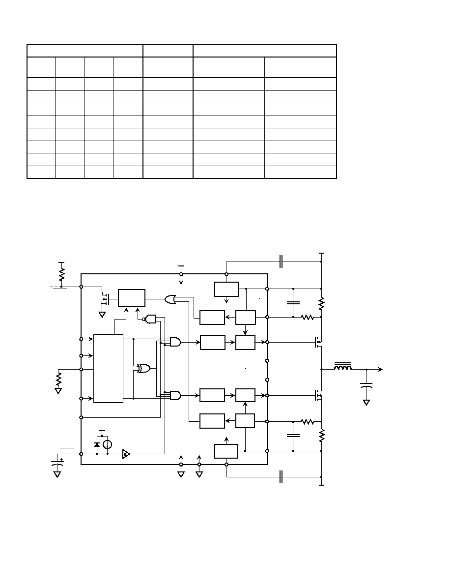
Block Diagram and Application Circuit
Ringer
Output
Rsense
Rsense
V
DD
Up
Translator
Down
Translator
Down
Translator
Up
Translator
P
Driver
N
Driver
Current
Trip
FAULT
P
IN
N
IN
RESET
De-glitcher
DEADBAND
ENABLE
MODE
V
DD
Control
Logic
V
NN1
V
PP1
SIG
GND
V
PP2
Regulator
V
NN2
Regulator
V
DD
Current
Trip
PWR
GND
+5V
NC
NC
V
PP1
V
PP2
V
PSEN
V
PGATE
V
NN1
V
NN2
V
NSEN
V
NGATE
Note: P
IN
, N
IN
, and ENABLE are internally pulled low. MODE is internally pulled high.
A Reset capacitor in the range of 1-10
µF will yield a couple-second turn-on delay. Tantalum is recommended.
10
µA
reset
clk
HV430
5
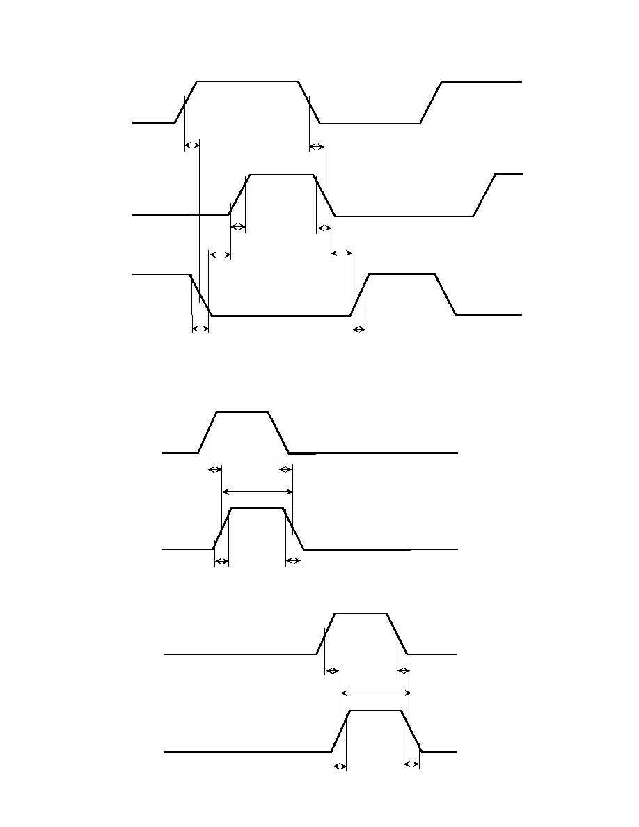
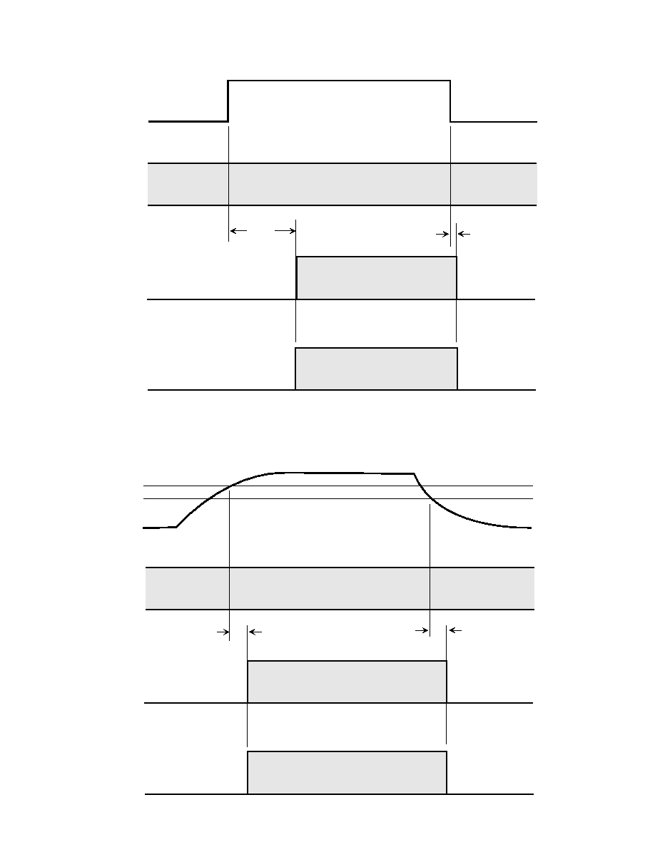
Single-Control Mode Timing
Dual-Control Mode Timing
t
Prise
t
N-Pdelay
t
P-Ndelay
t
Nrise
t
N-Pdeadband
N
IN
P
OUT
N
OUT
t
Pfall
t
Nfall
t
P-Ndeadband
OFF
ON
OFF
ON
V
NN1
V
NN2
V
PP1
V
PP2
0
1
GND
V
DD
t
Prise
t
Pdelay(on)
t
Pdelay(off)
t
Nrise
t
Nfall
t
Ndelay(on)
t
Ndelay(off)
P
IN
P
OUT
N
IN
N
OUT
t
Pfall
t
Ppulse(min)
t
Npulse(min)
OFF
ON
OFF
ON
V
NN1
V
NN2
V
PP1
V
PP2
GND
V
DD
GND
V
DD
0
1
0
1
HV430
6
ENABLE Timing
N
IN
/P
IN
P
OUT
N
OUT
OFF
ON
OFF
ON
V
NN1
V
NN2
V
PP1
V
PP2
0
1
GND
V
DD
ENABLE
0
1
GND
V
DD
t
EN(OFF)
t
EN(ON)
Off
Switching
Off
Switching
Off
Switching
Off
RESET Timing
N
IN
/P
IN
P
OUT
N
OUT
OFF
ON
OFF
ON
V
NN1
V
NN2
V
PP1
V
PP2
0
1
GND
V
DD
RESET
V
RESET(ON)
GND
t
RST(OFF)
t
RST(ON)
Off
Switching
Off
Switching
Off
Switching
Off
V
RESET(OFF)
HV430

7
FAULT Timing
N
IN
P
OUT
N
OUT
OFF
ON
OFF
ON
V
NN1
V
NN2
V
PP1
0
1
GND
V
DD
N
SENSE
FAULT
OK
Over
Note: N
sense
overcurrent shown. P
sense
operates identically.
ENABLE
or
RESET
0
1
GND
V
DD
V
PP2
t
FAULT(HOLD)
ENABLE or RESET
clears FAULT immediately
GND
V
DD
w/ext pull-up
HV430

8
Pin Description
V
PP1
Positive high voltage supply.
V
PP2
Positive gate voltage supply.
Generated by an internal linear regulator.
A 25V, 100nF capacitor should be
connected between V
PP2
and V
PP1
.
V
NN1
Negative high voltage supply.
V
NN2
Negative gate voltage supply.
Generated by an internal linear regulator.
A 25V, 100nF capacitor should be
connected between V
NN2
and V
NN1
.
V
DD
Logic supply voltage.
SGnd
Low voltage logic ground.
PGnd
High voltage power ground.
P
IN
Logic control input.
When mode is high, logic input high turns ON the external high voltage P-channel MOSFET.
Internally pulled low.
N
IN
Logic control input.
When mode is high, logic input high turns ON the external high voltage N-channel MOSFET.
Internally pulled low.
ENABLE
Logic enable input.
Logic high enables IC.
Internally pulled low.
MODE
Logic mode input.
0=single-control; 1=dual-control.
When MODE is high, N
IN
and P
IN
independently control N
OUT
and P
OUT
, respectively.
When MODE is low, N
IN
controls both outputs in a complementary manner.
(See Truth Table)
FAULT
Logic output.
Fault is at logic low when either current limit sense pin, V
Psen
or V
Nsen
, is activated.
Remains
active until overcurrent condition clears or ENABLE=0 or RESET=0.
RESET
Power-on reset. A capacitor connected between this pin and ground determines the delay time between application
of V
DD
and when the device outputs are enabled.
Low leakage tantalum recommended.
DEADBAND
A resistor between this pin and ground sets the `break-before-make' time between output transitions.
Applicable
only in single-control mode.
For minimum deadtime, a 5.6k resistor to ground should be used.
For dual-input
mode, tie to Vdd.
V
Pgate
Gate drive for external P-channel MOSFET.
V
Ngate
Gate drive for external N-channel MOSFET.
V
Psen
Pulse by pulse over current sensing for P-Channel MOSFET.
V
Nsen
Pulse by pulse over current sensing for N-Channel MOSFET.
Pin Configuration
1
10
2
3
4
5
6
7
8
9
20
11
19
18
17
16
15
14
13
12
top view
SOW 20
V
DD
Fault
Mode
P
IN
N
IN
Enable
Reset
Deadband
SGND
PGND
V
PP2
V
PP1
V
PSEN
V
PGATE
N/C
N/C
V
NGATE
V
NSEN
V
NN1
V
NN2
HV430
1235 Bordeaux Drive, Sunnyvale, CA 94089
TEL: (408) 744-0100 ∑ FAX: (408) 222-4895
www.supertex.com
12/13/010
©2001 Supertex Inc. All rights reserved. Unauthorized use or reproduction prohibited.