 | –≠–ª–µ–∫—Ç—Ä–æ–Ω–Ω—ã–π –∫–æ–º–ø–æ–Ω–µ–Ω—Ç: HV441 | –°–∫–∞—á–∞—Ç—å:  PDF PDF  ZIP ZIP |
1
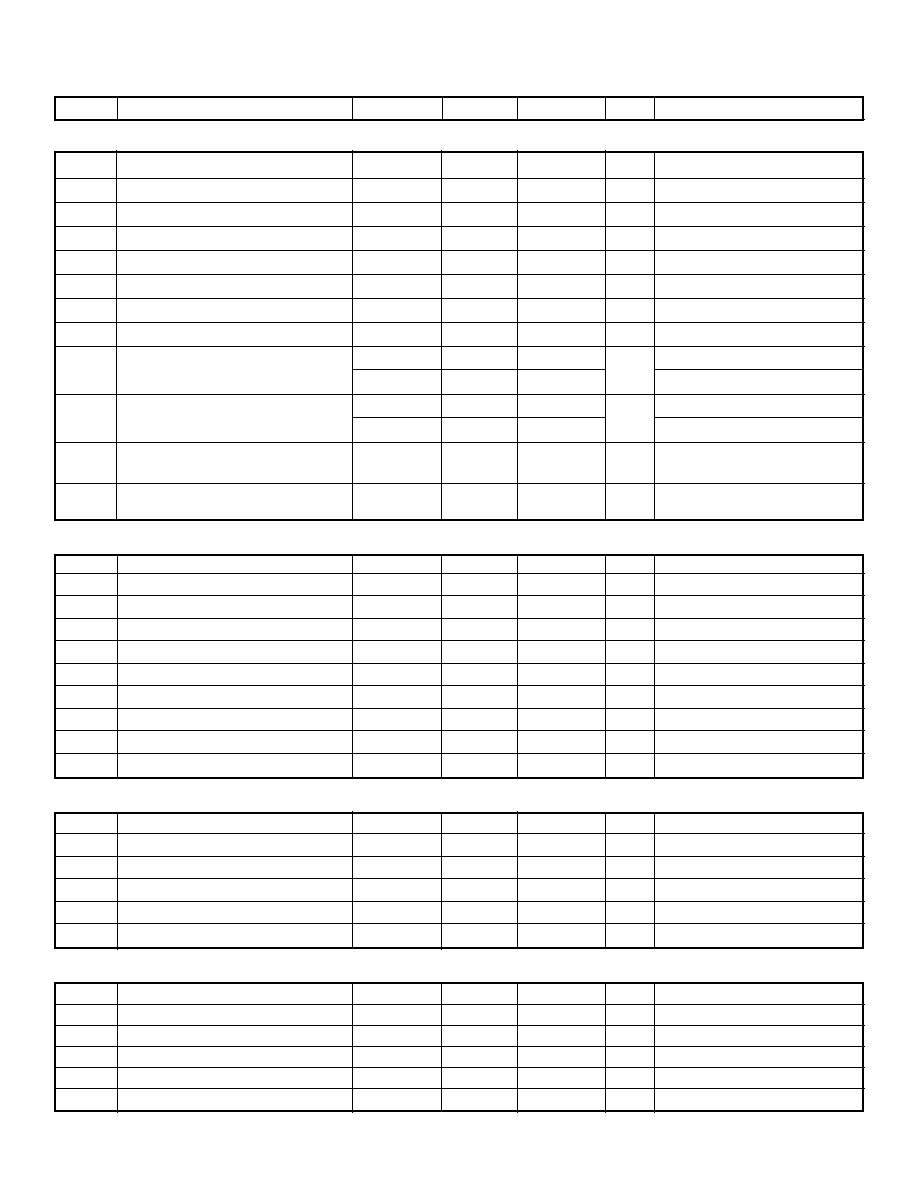
Absolute Maximum Ratings
V
PP1
- V
NN1
, power supply voltage
+240V
V
PP1
, positive high voltage supply
+120V
V
PP2
, positive gate voltage supply
+120V
V
NN1
, negative high voltage supply
-170V
V
NN2
, negative gate voltage supply
-170V
V
DD1
, low voltage logic supply
+7.5V
V
DD2
, low voltage analog/logic supply
+18V
Storage temperature
-65∞C to +150∞C
Power dissipation
1200mW
Operating Voltage
Package Options
V
PP1
- V
NN1
44-Pin PLCC
220V
HV441PJ
General Description
The Supertex HV441 is a monolithic integrated circuit capable of
generating up to a 70V RMS sine wave output at frequencies of
15Hz to 60Hz with a load of 5 North American RENs. Its output
rating can be enhanced to 20 North American RENs with the
addition of two Supertex MOSFETs: one N-Channel MOSFET,
the TN2524N8 and one P-Channel MOSFET, the TP2522N8. The
high voltage outputs have pulse by pulse over current protection
set by two external sense resistors.
The HV441 generates a low voltage reference sine wave by using
external passive components. An external sine wave signal can
be used if desired. The HV441 amplifies the reference sine wave
signal by pulse width modulating the high voltage output at a
nominal frequency of 100KHz. An error amplifier compares the
output sine wave with the reference sine wave and adjusts the
pulse width accordingly. Both the amplitude of the output sine
wave and the DC offset voltage are adjustable.
Ordering Information
High-Voltage Ring Generator
Applications
Stand alone high voltage ring generator
Set-top/Street box ring generator
Pair gain ring generator
Wireless local loops
Fiber in the loop/to the curb
Coax cable loop
For detailed circuit and application information, please
refer to application not AN-H35.
HV441
Features
220V maximum operating voltage
Integrated high voltage transistors
Up to 70 V
RMS
ring signal
Adjustable AC and DC output voltage level
Adjustable ring signal start phase angle
Pulse by pulse output over current protection
5 REN output capability
External MOSFETs enhance output rating to 20 REN
12/13/01
Supertex Inc. does not recommend the use of its products in life support applications and will not knowingly sell its products for use in such applications unless it receives an adequate "products liability
indemnification insurance agreement." Supertex does not assume responsibility for use of devices described and limits its liability to the replacement of devices determined to be defective due to
workmanship. No responsibility is assumed for possible omissions or inaccuracies. Circuitry and specifications are subject to change without notice. For the latest product specifications, refer to the
Supertex website: http://www.supertex.com. For complete liability information on all Supertex products, refer to the most current databook or to the Legal/Disclaimer page on the Supertex website.
2
Symbol Parameters
Min
Typ
Max
Unit
Conditions
V
osc1
Input voltage range for osc1
0
V
DD2
V
V
osc2
Input voltage range for osc2
0
V
DD2
V
V
oscin
Input voltage range for oscin
0
V
DD1
V
f
oscout
Output frequency of oscout
120
KHz
f
OSC1
= 480KHz
V
oscout
Oscout voltage
0
V
DD1
V
Oscillator
R
SOURCE
V
OUT
P source resistance
55
I
OUT
= 100mA
R
SINK
V
OUT
P sink resistance
55
I
OUT
= -100mA
DC
P
Max P-Channel duty cycle
92
%
V
PP1
= +60V, V
NN1
= -160V
DC
N
Max N-Channel duty cycle
94
%
V
PP1
= +60V, V
NN1
= -160V
td
(ON)
HV
OUT
delay time
150
ns
t
rise
HV
OUT
rise time
50
ns
td
(OFF)
HV
OUT
delay time
200
ns
t
fall
HV
OUT
fall time
50
ns
V
psen
HV
OUT
current source sense voltage
V
PP1
≠ 0.75
V
PP1
≠ 1.00
V
PP1
≠ 1.25
V
V
PP1
≠ 0.67
V
PP1
≠ 1.31
T
A
= -40∞C to +85∞C
V
nsen
HV
OUT
current sink sense voltage
V
NN1
+ 0.75
V
NN1
+ 1.00
V
NN1
+ 1.25
V
V
NN1
+ 0.65
V
NN1
+ 1.33
T
A
= -40∞C to +85∞C
t
shortP
HV
OUT
off delay time when current
100
ns
source sense is activated
t
shortN
HV
OUT
off delay time when current
100
ns
sink sense is activated
High Voltage Output
Symbol Parameters
Min
Typ
Max
Unit
Conditions
Electrical Characteristics
(Over operating supply voltage unless otherwise specified, T
A
= 25∞C.)
Comparator
Symbol Parameters
Min
Typ
Max
Unit
Conditions
V
OS
Input offset voltage
4
mV
I
IN
Input bias current
500
nA
V
IN
Input voltage range
V
DD2
≠ 2
V
A
V
Voltage gain
80
dB
t
res
Response time
80
ns
Operational Amplifier 1, 2, and 3
Symbol Parameters
Min
Typ
Max
Unit
Conditions
V
OS
Input offset voltage
5
mV
I
IN
Input bias current
500
nA
V
IN
Input voltage range
1
V
DD2
≠ 1
V
V
OUT
Output voltage swing
0.5
V
DD2
≠ 1
V
I
SOURCE
Output source current
3
mA
I
SINK
Output sink current
-2.75
mA
A
O
DC open loop gain
70
85
dB
BW
Bandwidth
100
KHz
SR
Output slew rate
0.3
V/µs
HV441

3
Pin Description
Symbol
Parameters
Min
Typ
Max
Unit
Conditions
V
PP1
High voltage positive supply
15
110
V
T
A
= -40∞C to +85∞C
V
PP2
Positive charge pump output voltage
V
PP1
≠ 8
V
PP1
≠ 19
V
T
A
= -40∞C to +85∞C
V
NN1
High voltage negative supply
V
PP
≠ 220
-110
V
T
A
= -40∞C to +85∞C
V
NN2
Negative charge pump output voltage
V
NN1
+ 5.2
V
NN1
+10.5
V
T
A
= -40∞C to +85∞C
V
DD1
Low voltage supply
3.0
5.5
V
T
A
= -40∞C to +85∞C
V
DD2
Low voltage supply
10.8
13.5
V
T
A
= -40∞C to +85∞C
I
PP1Q
V
PP1
quiescent current
250
400
µA
T
A
= -40∞C to +85∞C
I
NN1Q
V
NN1
quiescent current
250
500
µA
T
A
= -40∞C to +85∞C
I
PP1
V
PP1
operating current
0.8
mA
HV
OUT
switching at 100KHz,
V
PP1
= +60V, V
NN1
= -160V,
T A = -40∞C to +85∞C
I
NN1
V
NN1
operating current
1.0
mA
I
DD1Q
V
DD1
quiescent current
10
µA
I
DD2Q
V
DD2
quiescent current
4.0
mA
Electrical Characteristics, cont'd.
(Over operating supply voltage unless otherwise specified, T
A
= 25∞C.)
V
PP1
Positive high voltage supply
V
PP2
Positive gate voltage supply. Generated by an internal linear regulator.
V
NN1
Negative high voltage supply
V
NN2
Negative gate voltage supply. Generated by an internal linear regulator.
V
DD1
+3.3V to 5.0V supply for input and output logic
V
DD2
+12V supply for analog/logic circuit
GND
Low voltage ground
P
GND
High voltage power ground
Input1-
Inverting input of op-amp 1.
Input1+
Noninverting input of op-amp 1.
Output1
Output of op-amp 1.
Input2-
Inverting input of op-amp 2.
Input2+
Noninverting input of op-amp 2.
Output2
Output of op-amp 2.
Input3-
Inverting input of op-amp 3.
Input3+
Noninverting input of op-amp 3.
Output3
Output of op-amp 3.
V
ref
External input reference voltage for zero crossing detection.
On/Off
Enables/Disables HV
OUT
.
osc1
Input 1 for external resonator. Connect to GND when not in use.
osc2
Input 2 for external resonator. Leave floating when not in use.
oscin
External oscillator input. Zero to V
DD1
input signal. Connect to V
DD1
when not in use.
oscout
Oscillator output; 1/4 frequency of external resonator. 50% duty cycle.
HV
OUT
High voltage output. Voltage swings from V
PP1
to V
NN1
.
V
psen
Pulse by pulse over current sensing for internal P-Channel MOSFET.
V
nsen
Pulse by pulse over current sensing for internal N-Channel MOSFET.
P
gate
Gate drive for external P-channel MOSFET.
Ngate
Gate drive for external N-channel MOSFET.
HV441

4
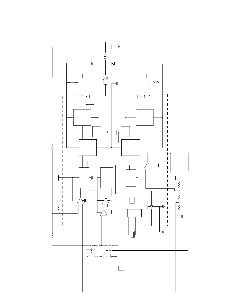
Functional Block Diagram
High
Voltage
Level
Translator
Pulse Width
Regulator
Output2
Input2-
Input2+
Input1-
Input1+
Input3-
Input3+
Output3
Output1
op-amp2
op-amp1
op-amp3
comp
˜4
OSC
osc1
osc2
osc in
osc out
GND
V
DD1
V
DD2
V
DD2
V
DD2
V
DD2
V
DD2
V
REF
V
DD1
Zero Voltage
Crossing
Detection
Ramp
Generator
Linear
Reg
V
PP1
V
DD2
V
psen
V
pgate
V
PP2
HV
OUT
P
GND
Current
Sense
and
Driver
Current
Sense
and
Driver
Linear
Reg
V
NN2
V
nsen
V
ngate
V
NN1
+
≠
+
≠
-
+
-
+
ON/OFF
High
Voltage
Level
Translator
HV441
5
High
Voltage
Level
Translator
Pulse Width
Regulator
Output2
Input2-
Input2+
Input1-
Input1+
Input3-
Input3-
Output3
Output1
op-amp2
op-amp1
op-amp3
205K
On = 5V
Off = 0V
39nF
39nF
25.5K
8.2K
8.2nF
12V
1M
comp
˜
4
OSC
osc1
osc2
osc in
osc out
GND
V
DD1
V
DD2
V
DD2
V
DD2
45.3K
12V
158K
205K
400KHz
V
DD2
V
DD2
V
REF
V
DD1
Zero Voltage
Crossing
Detection
Ramp
Generator
Linear
Reg
V
PP1
= +60V
V
DD2
V
psen
V
pgate
V
PP2
HV
OUT
P
GND
4.3
4.3
0.1
µ
F
0.22
µ
F
Sine Wave
Ring Output,
20Hz
Current
Sense
and
Driver
Current
Sense
and
Driver
Linear
Reg
V
NN2
V
nsen
V
ngate
V
NN1
= -160V
0.1
µ
F
25V
+
≠
+
≠
≠
+
-
+
5.0V
21K
205K
15K
10.7K
High
Voltage
Level
Translator
BAS21
1.5mH
BAS21
Typical 5 REN Application Circuit
HV441

6
Typical 20 REN Application Circuit
High
Voltage Level Translator
Pulse
Width
Regulator
Output2
Input2-
Input2+
Input1-
Input1+
Input3-
Input3-
Output3
Output1
op-amp2
op-amp1
op-amp3
205K
O
n=5
V
Of
f=0V
39nF
39nF
25.5K
8.2K
2.2nF
12V
1M
comp
˜
4
OSC
osc1
osc2
osc
in
osc
out
GND
V
DD1
V
DD2
V
DD2
V
DD2
45.3K
12V
158K
205K
400KHz
V
DD2
V
DD2
V
REF
V
DD1
Zero
Voltage
Crossing Detection
Ramp
Generator
Linear Reg
V
PP1
=
+60V
V
DD2
V
psen
V
pgate
V
PP2
HV
OUT
P
GND
1.0
1.0
0.47
µ
F
Sine
Wave
Ring
Output,
20Hz
Current Sense
and Driver
Current Sense
and Driver
Linear Reg
V
NN2
V
nsen
V
ngate
TN2524N8
TP2522N8
V
NN1
=
-160V
0.1
µ
F
0.1
µ
F
25V
+
–
+
≠
–
+
-
+
5.0V
21K
205K
15K
10.7K
High
Voltage Level Translator
BAS21
BAS21
220
µ
H
HV441

7
Pin Configuration
Package Outline
6
40
41
42
43
44
1
2
3
4
5
39 38 37 36 35 34 33 32 31 30 29
18
28
27
26
25
24
23
22
21
20
19
7
8
9
10 11 12 13 14 15 16 17
HV441
Pin Function
1
N/C
2
N/C
3
N/C
4
V
ref
5
N/C
6
V
DD2
7
N/C
8
V
DD1
9
osc1
10
osc2
11
oscin
12
oscout
13
ON/OFF
14
N/C
15
N/C
16
N/C
17
V
NN1
18
N/C
19
V
NN2
20
N
gate
21
V
nsen
22
N/C
Pin Function
23
HV
OUT
24
N/C
25
V
psen
26
P
gate
27
V
PP2
28
N/C
29
V
PP1
30
N/C
31
N/C
32
N/C
33
P
GND
34
GND
35
Output2
36
Input2-
37
Input2+
38
Output1
39
Input1-
40
Input1+
41
Output3
42
Input3-
43
Input3+
44
N/C
top view
44-pin PLCC
HV441
1235 Bordeaux Drive, Sunnyvale, CA 94089
TEL: (408) 744-0100 ∑ FAX: (408) 222-4895
www.supertex.com
12/13/010
©2001 Supertex Inc. All rights reserved. Unauthorized use or reproduction prohibited.