 | –≠–ª–µ–∫—Ç—Ä–æ–Ω–Ω—ã–π –∫–æ–º–ø–æ–Ω–µ–Ω—Ç: HV461FG | –°–∫–∞—á–∞—Ç—å:  PDF PDF  ZIP ZIP |

Supertex Inc. does not recommend the use of its products in life support applications and will not knowingly sell its products for use in such applications unless it receives an adequate
"products liability indemnification insurance agreement." Supertex does not assume responsibility for use of devices described and limits its liability to the replacement of devices determined
to be defective due to workmanship. No responsibility is assumed for possible omissions or inaccuracies. Circuitry and specifications are subject to change without notice. For the latest
product specifications, refer to the Supertex website: http://www.supertex.com. For complete liability information on all Supertex products, refer to the most current databook or to the
Legal/Disclaimer page on the Supertex website.
HV461FG Ring Generator Controller IC
Features
3.3V operation, logic inputs 3.3V & 5V compatible
Digital control of ring frequency, amplitude, and offset
Control via 8-bit bus or via individual inputs
8 built-in ring frequencies: 16
2
/
3
, 20, 25, 33
1
/
3
, 40, 50,
60Hz
External ring frequency input
Low distortion sine wave synthesizer
AC-only, AC+DC, or DC-only ringer output
Adjustable over-current protection
Internal precision voltage references
Power-on reset and undervoltage lockout for hotswap
capability
Sync output with adjustable lead time for synchronizing
ringing relays
Fault output for problem detection
Open or closed loop operation
Efficient 4-quadrant operation
Zero-cross turn-on with zero-cross turn-off option
Applications
PBX
DLC
Key Systems
Remote Terminal
Wireless Loop Systems
Description
The HV461FG is a highly integrated Ring Generator
controller IC designed to work with a patented four-quadrant
inverter topology, with Synchronous Rectifiers on the
secondary side to achieve higher efficiencies. The inverter
delivers the desired ring voltage from a standard -48V
Telecom power supply.
HV461 consists of a sine wave synthesizer that can provide
eight different ring frequencies for universal applications.
Any other frequency in the 12 to 63 Hz range can be
obtained by applying an external logic signal to the IC. A
transparent latch permits control of the ringer output through
the 8-bit bus or individually. The output amplitude and DC
offset can be digitally controlled providing high flexibility to
the designers. The patented inverter topology using the
HV461 controller IC is capable of achieving higher
efficiencies, typically over 80%, and drive up to a 40 REN
load.
The controller allows ring generators to provide a floating
94VAC (rms) waveform that can be referenced to either the
≠48V or any other offset level by using the programmable
offset pins of the IC. Output offset may be achieved by
directly generating the offset within the power stage, or by
floating the output stage on a DC source, or both.
HV461 also has an internal Boost Converter that can be
used to provide the gate drive voltages for the two
MOSFETS on the primary side and the two secondary
rectifiers on the secondary side.
HV461
Initial Release
Typical Application

HV461
2
Specifications
(unless otherwise specified: V
DD
= +3.3V, T
A
= -40∫C to +85∫C)
External Supply
Symbol Parameter
Min
Typ
Max Unit
Conditions
V
DD
Supply
Voltage
3.0 3.3 3.6 V
I
DD
Supply Current
(AVDD + DVDD)
7 30
mA
f
PWM
=100kHz
f
osc
=19.6608MHz SW
outputs NC
Open loop config
External V
GD
Gate Drive Supply
Symbol Parameter
Min
Typ
Max
Unit
Conditions
V
GD
Boost circuit voltage
9.0
9.6
10.2
V
I
GD
Gate drive supply
current
5
10
mA
mA
V
DD
=2.97-3.63V, SW outputs unloaded
V
DD
=2.50-2.93V, SW outputs unloaded
V
DR(lo)
Drive voltage, low
0.2
V
I
OUT
=-10
µ
A
V
DR(hi)
Drive voltage, hi
V
DD
-0.4 V
I
OUT
=10
µ
A
t
RISE
Rise
time
100
ns
C
L
=200pF
t
FALL
Fall
time
100
ns
C
L
=200pF
f
GD
Converter frequency
same as PWM
D
GD
Duty
cycle
45 50
55 %
Voltage Reference
Symbol Parameter
Min Typ Max Unit
Conditions
V
REF1
Reference voltage 1
1.237
1.250
1.263
V
T
a
=25∫C
TC
REF1
Temperature
coefficient
200
µV/∫C
V
ref1
Output regulation
-6.25
+6.25
mV
I
out
=±100
µ
A
V
REF2
Reference voltage 2
2.475
2.500
2.525
V
T
a
=25∫C
TC
REF2
Temperature
coefficient
500
µV/∫C
V
ref2
Output regulation
-12.5
0
mV
I
out
=0≠100
µ
A source
Absolute Maximum Ratings
V
DD
+4.0V
Digital Inputs
-0.5V to +7.0V
Analog Inputs
-0.5V to +7.0V
Storage Temperature
-65∞C to +150∞C
Operating Temperature
-40∞C to +85∞C
Ordering Information
Package Option
Order Number
48 lead TQFP
HV461FG

HV461
3
Logic Inputs
Symbol Parameter
Min Typ Max
Unit
Conditions
V
IN(lo)
Input voltage low
0.3∑V
DD
V
V
IN(hi)
Input voltage high
0.7∑V
DD
V
I
IN(lo)
Input current low
-1
µ
A
V
IN
=0V
I
IN(hi)
Input current high
1
µ
A
V
IN
=5.0V
C
IN
Input
capacitance
10 pF
t
S
Set-up
time
100 ns
t
H
Hold
time
100 ns
RESET
Symbol Parameter
Min
Typ
Max
Unit
Conditions
V
RESET(ON)
RESET on voltage
1.200
1.325
1.450
V
V
RESET(OFF)
RESET off voltage
1.000
1.125
1.250
V
V
RESET (HYS)
RESET
hysteresis
0.150 0.200 0.250 V
I
P-UP
RESET pull-up current
7.0
10.0
13.0
µ
A
Undervoltage Lockout
Symbol Parameter
Min
Typ
Max
Unit
Conditions
V
DD(ON)
V
DD
on voltage
2.75
2.85
2.95
V
V
DD(OFF)
V
DD
off voltage
2.60
V
V
DD(HYS)
V
DD
hysteresis
0.10
V
V
GD(ON)
V
GD
on voltage
same as V
GD
regulation point
V
V
GD(OFF)
V
GD
off voltage
7.0
V
V
GD(HYS)
V
GD
hysteresis
0.20
V
Fault Output
Symbol Parameter
Min
Typ
Max
Unit
Conditions
V
OUT(lo)
Output voltage low
0.2
V
I
OUT
=1mA
K
FAULT(on)
FAULT on threshold
6
8
10
%*
C
FAULT
=10
µ
F
K
FAULT(off)
FAULT off threshold
1
2
3
%*
C
FAULT
=10
µ
F
t
FAULT(hold)
FAULT hold time
50
mS
C
FAULT
=10
µ
F
*
Percent of time PWM overrange or overcurrent is active.
Amplifiers
Symbol Parameter
Min Typ Max
Unit
Conditions
V
IN
Input
Range
0.25
2.50 V
I
IN
Input Bias Current
-500
500
nA
V
IN
=0.5V to V
DD
-0.5
V
OFFSET
Input Offset Voltage
-5
5
mV
V
OUT(min)
Min
output
0.1
0.2
V I
OUT
=±100uA
V
OUT(max)
Max
output
V
DD
-0.2
V
DD
-0.1
I
OUT
=±100uA
A
VOL
Open Loop Gain
60
80
dB
CMRR
Common mode rejection ratio
-40
-60
dB

HV461
4
GBW Gain-Bandwidth
Product
1
MHz
SL Slew
Rate
0.1
V/
µ
s
PSRR
Power supply rejection ratio
-30
dB
f<10kHz
Sinewave Synthesizer
Symbol Parameter
Min Typ Max Unit
Conditions
V
DC
DC
level
1.237 1.250 1.263 V
A Amplitude
1.940
2.000
2.060
0
V
P-P
V
P-P
AMP
00
AMP=00
f
0
Frequency
16
2
/
3
Hz
FREQ=000,
f
OSC
=19.6608MHz
f
1
Frequency
20
Hz
FREQ=001,
f
OSC
=19.6608MHz
f
2
Frequency
25
Hz
FREQ=010,
f
OSC
=19.6608MHz
f
3
Frequency
30
Hz
FREQ=011,
f
OSC
=19.6608MHz
f
4
Frequency
33
1
/
3
Hz
FREQ=100, f
OSC
=19.6608MHz
f
5
Frequency
40
Hz
FREQ=101,
f
OSC
=19.6608MHz
f
6
Frequency
50
Hz
FREQ=110,
f
OSC
=19.6608MHz
f
7
Frequency
60
Hz
FREQ=111,
f
OSC
=19.6608MHz
f
Frequency accuracy
0.1
%
f
osc
=19.6608MHz
THD Harmonic
distortion
3
% C
SINE
=33nF
f
ring
=16
2/3
to 60Hz
R
OUT
Output
resistance
14.4
72.0
16.0
80.0
17.6
88.0
k
k
AMP
00
AMP=00
External Ring Frequency
Symbol Parameter
Min Typ Max Unit
Conditions
f
CAP(lo)
Capture frequency low*
12
Hz
loop filter=(33
µ
F+10k
)||4.7
µ
F
f
CAP(hi)
Capture frequency high*
63
Hz
loop filter=(33
µ
F+10k
)||4.7
µ
F
V
IN(lo)
Input
low
0.3∑V
DD
V
V
IN(hi)
Input
high
0.7∑V
DD
V
RING
Phase jitter, sine ref out
-5
+5
deg
loop filter=(33
µ
F+10k
)||4.7
µ
F
* Lock range is the same as capture range
Sine Reference Attenuator
Symbol Parameter
Min Typ
Max Unit
Conditions
V
DC
DC
level
1.237 1.250 1.263
V V
IN(DC)
=1.250V
A
OFF
Attenuation
0.010 V/V
AMP=00
A
LO
Attenuation
0.495 0.500 0.505 V/V
AMP=01
A
MED
Attenuation
0.742 0.750 0.758 V/V
AMP=10
A
HI
Attenuation
0.990 1.000 1.010 V/V
AMP=11
V
IN
Input
range
0.2
V
DD
-0.2V V
DC REF Multiplexer
Symbol Parameter
Min Typ Max Unit
Conditions
V
IN
Input
range
0.0
V
DD
V
I
IN
Input bias current
-500
+500
nA
I
OFF
Off leakage current
1.0
µ
A
V
IN
= 0.5 to V
DD
-0.5V

HV461
5
ENABLE and SYNC
Symbol Parameter
Min
Typ
Max
Unit
Conditions
V
OUT(lo)
SYNC output voltage low
0.2
V
I
OUT
= 1mA sink
V
OUT(hi)
SYNC output voltage high
V
DD
- 0.2
V
I
OUT
= 1mA source
t
ON
ENABLE delay, on
5
µ
s
t
OFF
ENABLE delay, off
0
60
1
µ
s
ring cycle
SYNCMODE=0
SYNCMODE=1
SYNC(ON)
SYNC on lead time
4.5
5
5.5
ms
C
SINE
=0
R
SYNC
=154k
C
SYNC
=47nF
SYNC(OFF)
SYNC off delay
-250
0
+250
µ
s
C
SINE
=10nF
t
SYNC(rise)
SYNC rise time
300
ns
C
L
=50pF
t
SYNC(fall)
SYNC fall time
300
ns
C
L
=50pF
PWM Controller
Symbol Parameter
Min Typ
Max
Unit
Conditions
PWM Frequency
f
PWM
PWM
frequency
21.25
127.5
25.00
150.0
28.75
172.5
kHz
kHz
R
PWM
=500k
R
PWM
=83k
t
PWMSYNC(OUT)
PWM sync output pulse
width
30 50 70 ns
t
PWMSYNC(IN)
PWM sync input pulse width
25
ns
f
PWMSYNC(IN)
PWM sync input frequency
range
25 150
kHz
V
PWMSYNC(lo)
PWM sync output low
voltage
0.2
V
I
OUT
=1mA sink
I
PWMSYNC
PWM sync pull-up current
100
µ
A
Switch Driver Outputs
V
OUT(lo)
Output voltage, low
0.2
V
I
OUT
=20mA sink
V
OUT(hi)
Output voltage, high
V
GD
-0.2
V
I
OUT
=20mA source
t
RISE
Rise
time
50 ns
C
L
=4nF
t
FALL
Fall
time
50 ns
C
L
=4nF
Timing
D Duty
cycle
23
48
73
25
50
75
27
52
77
%
%
%
PWMin=0.625V
PWMin=1.250V
PWMin=1.875V
V
DCL
=0V
D
limit
Duty cycle limit
12
72
22
62
20
80
30
70
28
88
38
78
%
%
%
%
V
DCL
= 0.50V, PWM
IN
=0V
V
DCL
= 0.50V, PWM
IN
=2.5V
V
DCL
= 0.75V, PWM
IN
=0V
V
DCL
= 0.75V, PWM
IN
=2.5V
I
DCL
V
DCL
input current
1
µ
A
V
DCL
=0-1V
t
DB
Primary switch deadband
0
0.95
100
1.00
150
1.05
ns
µ
s
C
DB
=0pF
R
DB
=14k
, C
DB
=100pF
t
DLY
Secondary switch delay
0
0.95
100
1.00
150
1.05
ns
µ
s
C
DLY
=0pF
R
DLY
=14k
, C
DLY
=100pF
HV461
6
Switch Outputs
ENABLE AMP OFF SW1 SW2 SW3 SW4
0 00
XX
Off
Off
Off
Off
0
00
XX Off Off
Switching
Switching
1 XX
XX
Switching
Switching
Switching
Switching
X = don't care,
00 = 01,10, or 11
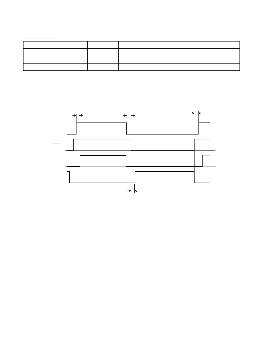
Switch Timing
SW1
t
DB
SW2
SW3
SW4
t
DB
t
DLY
On
Off
Off
On
On
Off
Off
On
t
DLY
Figure 1: Switch Timing Diagram

HV461
7
ENABLE and SYNC Timing: SYNCMODE=0
ENABLE
SYNC
t
ON
SYNC(ON)
SINE REF
ErrAmp
Siezed
Siezed
Free
t
OFF
Decay time
dependent on
value of cap
connected to
SINEREF.
ENABLE and SYNC Timing: SYNCMODE=1
ENABLE
SYNC
t
ON(delay)
SYNC(ON)
Filtered
SINE REF
sync at 0∫ or 180∫
ErrAmp
Siezed
Siezed
Free
SYNC(OFF)
Figure 2: ENABLE and SYNC Timing ≠ SYNCMODE=0
Figure 3: ENABLE and SYNC Timing ≠ SYNCMODE=1

HV461
8
AMP Timing
SYNC
t
SYNC(delay)
SYNC(ON)
SINE REF
AMP
AMP 00
AMP 00
AMP 00
AMP 00
amplitude changes
sync'd to zero crossings
Figure 4: AMP Timing
Typical Application
Figures 5 and 6 on pages 9 and 10 show the
schematic of a typical 15 REN ring generator
application. The basic design equations for elements
connected to different pins are given in the Pin
Descriptions Table beginning on page 11.

HV461
9
Block Diagram and Typical Application
Figure 5: Block Diagram and Typical Application
V
GD
FAULT
VREF1
ringer
output
SYNC
V
DD
RESET
3
DCREF1≠3
OSC
Sine Wave
Synthesizer
2
freq
2
AGND
DVDD
reset
SINEREF
Differential
Amplifier
Error
Amplifier
output
reference
Boost
Converter
SYNCMODE
Enable
Control
enable
PWMSYNC
SW
1
SW
2
SW
3
SW
4
sync
FRING
VGD
clk
LE
VDCL
VREF1
PLL
20k
VREF2
Precision
Reference
VREF1
DGND
PWM
Controller
PWMin
enable
overcurrent prideadband
sec delay
switch
drivers
current
limit
dutycyclelimit
osc
ROSC
freq
amp
offset
overrange
CL-
CL+
CLCOMP
Sync
VREF2
TSYNC
VREF1
20k
20k
40k
10k
20k
10k
VREF1
PGND
AVDD
XTAL
V
DD
VDR
DIFFAMP+
DIFFAMPO
DIFFAMP-
PLLFLT
TDB
TDLY
V
REF1
COMP1
COMP2
V
REF1
FREQ0
FREQ1
FREQ2
AMP0
AMP1
OFF0
OFF1
ENABLE
+1
10 A
Undervoltage
Detector
undervoltage
Latch
Offset
Mux
Amplitude
Mux
Deglitcher
CFAULT
referto power
stage schematic
V
DD
V
DD
2
+1
1.25V
2.50V
T
r
a
n
s
p
a
r
e
n
t
L
a
t
c
h
referto
power stage
schematic
V
DD
R
FAULT
100
V
DD
to host
controller
V
DD
external ring
frequency
C
PLL2
33µF
R
PLL
10k
C
PLL1
4.7µF
PLL filter only required for
external ring frequency
to host
controller
C
DLY
selected for
desired Fault
response time
R
FB2
4.02M
R
DB
4.7
C
DB
120pF
R
DLY
4.7
C
DLY
120pF
C
FAULT
10µF
R
DCL1
100
R
DCL2
33
R
OSC
267k
R
FB3
30.1k
R
FB1
30.1k
R
FB4
4.02M
C
COMP2
1nF
C
COMP1
47nF
R
COMP
2.7k
R
DC1
R
DC2
R
DC3
R
DC4
R
TSYNC
3.3k
C
TSYNC
100nF
Y
1
19.6608MHz
C
RESET
4.7µF
C
REF1
100nF
C
REF2
100nF
C
DD1
10µF
L
GD
330µH
D
GD
4148
Q
GD
TN2504
C
GD
6.8µF
C
SINE
47nF
C
DD2
100nF
C
DC
100nF
R
DC1
- R
DC4
selected for
the desired DC Offsets.
R
TSYNC
and C
TSYNC
selected for
desired ring sync lead time
k
k
k
k
k
HV461FG

HV461
10
Typical Power Stage for 15 REN Ring Generator
-48V
SW
2
SW
1
SW
3
SW
4
CL-
CL+
CLCOMP
PWR
GND
V
REF1
Output
Reference
Ringer
Output
R
OUT2
1.0M
52 H
Q
SW2
IRF9540
Q
SW1
IRF530
C
IN1
470µF
C
IN2
470nF
R
PR1
100k
R
SW1a
220
D
SW2
MMBD4148
Z
SWa,b
12V
C
PRI2
470nF
R
PRI2
100k
C
PRI1
100µF
C
PRI3
100µF
C
PRI4
470nF
T
MAIN
1:6.5:6.5
C
SW4b
100nF
C
OUT1
1µF
C
OUT2
1µF
Q
SW3
IRFR320
Q
SW4
IRFR320
R
OUT1
1.0M
R
SW4a
10k
R
SW4b
220
D
SW4
MMBD4148
R
SW3b
10k
D
SW3
MMBD4148
R
SW3a
220
C
SW3b
100nF
Z
SW2a,b
12V
R
SW2a
220
D
SW2
MMBD4148
L
IN
Ferrite bead
R
SENSE
0.18
R
CL3
39k
R
CL2
10k
R
CL1
10k
R
CL4
6.8k
C
CL2
68nF
C
CL1
10nF
C
SW3a
100nF
C
SW4a
100nF
C
SW1
100nF
C
SW2
100nF
T
SW4
1:1
T
SW3
1:1
R
SW1b
100k
R
SW2b
100k
Figure 6: Typical Power Stage for 15 REN Ring Generator

HV461
11
Pin Descriptions
CL+
DVDD
VDR
SW1
SW2
VGD
PGND
SW3
SW4
DGND
TDB
TDLY
DCREF3
VREF1
VREF2
AVDD
TSYNC
XTAL
FRING
PLLFLT
ROSC
PWMSYNC
CFAULT
D
C
R
E
F
2
D
C
R
E
F
1
V
D
C
L
A
G
N
D
S
I
N
E
R
E
F
C
O
M
P
1
C
O
M
P
2
D
I
F
F
A
M
P
O
D
I
F
F
A
M
P
-
D
I
F
F
A
M
P
+
C
L
C
O
M
P
C
L
-
S
Y
N
C
M
O
D
E
S
Y
N
C
F
A
U
L
T
E
N
A
B
L
E
O
F
F
0
O
F
F
1
A
M
P
0
A
M
P
1
F
R
E
Q
0
F
R
E
Q
1
F
R
E
Q
2
HV461
RESET
L
E
Pin Name
Description
1
DCREF3
See DCREF1 and DCREF2 (pins 47 & 48).
2
VREF1
Outputs a 1.25V nominal reference voltage. Bypass with a 100nF capacitor to ground.
3
VREF2
Outputs a 2.50V nominal reference voltage. Bypass with a 100nF capacitor to ground.
4
AVDD
Supply for the analog section. 3.0 to 3.6V Must be from the same source as DVDD. Bypass with a 100nF
capacitor to ground as close as possible to the IC.
5
TSYNC
An RC network connected to this pin determines the SYNC pulse lead time (see SYNC pin 14). t
LEAD
= 0.48RC
If unused, this pin should be left unconnected.
6
XTAL
A crystal from this pin to ground provides the frequency reference for the internal sine wave synthesizer. A
19.6608MHz baud rate crystal provides the 8 most common ring frequencies. The crystal is operated in the
series mode. A loading capacitor is not necessary. See also FREQ0≠2 (pins 21≠23) and FRING (pin 7).
7
FRING
Ring frequency is normally selected from the 8 built-in frequencies using control inputs FREQ0≠2. Other
arbitrary frequencies in the range of 12 to 70Hz may be obtained by applying an external signal to FRING. This
external signal sets the ring frequency at a 1:1 ratio. The ring signal remains a sine wave, with amplitude and
offset still controlled via AMPx and OFFx. The ring signal, while frequency locked to the FRING signal, is not
phase≠synchronized to it. This allows the ring signal to immediately start at 0∫ when enabled via ENABLE or
AMP
00. When unused, this input must be connected to V
GD
.
8
PLLFLT
Phase locked loop filter. An RC network connected to this pin stabilizes the PLL that locks on to the optional
external ring frequency signal. (See FRING, pin 7) The RC network determines the lock time of the PLL. Due
to the low frequencies involved, it may take a couple seconds to lock to the external signal. See the typical
application schematic for typical values. When unused, this pin should be left unconnected.
9 ROSC
A resistor from this pin to V
DD
sets the PWM frequency. f
PWM
12.5GHz
/ R
OSC
(valid for 20-150kHz)
10
RESET
A capacitor from this pin to ground provides a power≠on reset interval. It has an internal 10
µ
A pull≠up to
charge the external reset capacitor. Alternatively, an external logic≠level or open≠drain signal may be applied
to implement the reset function. During the reset interval when V
RESET
<1.325V, the ringer output is disabled
regardless of the state of the ENABLE input, allowing time for the host controller to assume control. Use a low
leakage tantalum or ceramic capacitor. t
RESET
= 1.325V ∑ C
RESET
/ 10
µ
A
11 PWMSYNC This pin functions as both an input and an output. It is open≠drain with an internal 100
µ
A pull≠up. As an
output, it provides a short, low≠going pulse at the internal PWM frequency. As an input, it synchronizes internal
PWM frequency to the externally applied signal, provided the external signal is at a higher frequency. The low-
going applied sync pulse should be between 25ns and less than the PWM period in duration. The external
source should be open drain. If the PWMSYNC pins of multiple HV461s are tied together, their PWM
frequencies will be phase≠locked to the HV461 with the highest free-running frequency. A maximum of 10
HV461s may be tied together. If unused, this pin should be left unconnected.

HV461
12
12 CFAULT
A capacitor from this pin to ground sets the integration time of the FAULT detection circuitry. A larger capacitor
provides less suseptability to transient problems, while a smaller capacitor provides quicker response. Values
in the range of 1µF to 100µF are appropriate. If the FAULT output is not used, this pin should be grounded.
See also FAULT (pin 15).
13 SYNCMODE With SYNCMODE low, ringer output ceases the instant ENABLE goes low. When high, ringer output ceases at
the next ring signal phase crossing (0∫/180∫) after ENABLE goes low.
14 SYNC
Outputs a pulse indicating sine reference 0∫ and 180∫ phase crossing (not to be confused with zero≠voltage
crossing). The rising edge precedes phase crossing by a user≠adjustable time period (see TSYNC pin 44).
Falling edge coincides with sine reference phase crossing. SYNC is digitally derived, therefore phase shifts
caused by the external filter capacitor at SINEREF will not be reflected at the SYNC output.
15
FAULT
Indicates abnormal operating conditions of output overcurrent, supply undervoltage (V
DD
& V
GD
), or PWM
overrange (duty cycle limit ≠ see VDCL, pin 3). Together, these 3 conditions catch most any problem. When an
overcurrent or overrange condition exists for more than 8% of the time, this output becomes active. It is cleared
when the problem occurs less than 2% of the time. Undervoltage conditions immediately activate the FAULT
output. It is active low and open drain to allow wire-ORing. See CFAULT (pin 15) for additional information.
16 ENABLE
Ringer output enable. Active high. When enabled, the ring signal always starts immediately at 0 degrees. If
AMP00, SW1 and SW2 are held off when ENABLE=0 but SW3 and SW4 continue switching. If AMP=00, SW3
and SW4 are held off as well. When disabled, the error amplifier is set at unity gain to prevent saturation,
reducing turn-on glitches when re-enabled. See SYNCMODE (pin 13) for additional information.
17 OFF0
Sets ring DC offset. Offset changes are effected at the next phase crossing (0∫/180∫) of the ring signal. Except
for 00, offsets are set by the voltages at DCREF1≠3. (OFF0 is LSB) Offset = Ω x Gain x (V
DCREFx
- V
REF1
)
18 OFF1
00 = 0V
01 = DCREF1
10 = DCREF2
11 = DCREF3
19 AMP0
Sets ring amplitude. Amplitude changes are effected at the next phase crossing (0∫/180∫) of the ring signal.
Amplitudes, as a percentage of full scale, are: (AMP0 is LSB) Full scale amplitude = 0.707V
RMS
x Gain
20 AMP1
00 = 0%
01 = 50%
10 = 75%
11 = 100%
21 FREQ0
Sets ring frequency. Frequency changes are effected at the next phase crossing (0∫/180∫) of the ring signal.
Frequencies when using a 19.6608MHz crystal are: (FREQ0 is LSB)
22 FREQ1
000 = 16.7Hz
001 = 20Hz
010 = 25Hz
011 = 30Hz
23 FREQ2
100 = 33.3Hz
101 = 40Hz
110 = 50Hz
111 = 60Hz
24
LE
Latch enable. The latch gates control inputs FREQ0≠2, AMP0≠1, OFF0≠1, and ENABLE. When LE is high,
latch outputs follow inputs. On a low≠going transition, outputs are latched.
25 TDLY
An RC network on this pin sets the primary to secondary switch delay. This prevents the secondary≠side
switches (SW3&4) from turning on prematurely. t
DLY
=0.48RC
26 TDB
An RC network on this pin sets the deadband (break≠before≠make time) on the primary≠side switches
(SW1&2). Deadband prevents both switches from conducting simultaneously. t
DB
=0.48RC
27 DGND
Digital ground. Connect to AGND and PGND close to the IC.
28 SW4
Secondary≠side switch driver output.
29 SW3
Secondary≠side switch driver output.
30
SW2
Primary≠side N-channel switch driver output.
31 SW1
Primary≠side P-channel switch driver output.
32 PGND
Power ground. Connect to AGND and DGND close to the IC.
33 VGD
Supply for the SW1≠4 drivers. An external boost converter controlled by VDR provides 9.6V for driving the
power stage MOSFETs. An undervoltage condition on this supply pin disables ringer output and activates the
FAULT output.
34 VDR
Gate drive for the external boost converter circuit. Outputs a fixed 50% duty cycle at the ringer PWM frequency
(see ROSC, pin 9). Output voltage regulation is via burp-mode operation. This output is boostrapped to VGD,
thus during startup VDR amplitude is VDD and after startup is VGD. (See VGD, pin 33)
35 DVDD
Supply for the digital section. 3.0V to 3.6V input. Undervoltage disables ringer output. Must be from the same
source as AVDD. Bypass with a 100nF capacitor to ground as close as possible to the IC. An undervoltage
condition on this supply pin disables ringer output and activates the FAULT output.
36 CL+
Current limit amplifier non-inverting input.
HV461
13
37 CL-
Current limit amplifier inverting input.
38 CLCOMP
Current limit compensation. An RC network connected between this pin and CL- establishes current limit
reaction time and stability.
39 DIFFAMP+
Differential amplifier non-inverting input.
The differential amplifier sets gain, establishing output
40 DIFFAMP-
Differential amplifier inverting input.
amplitude and DC offset in conjunction with AMPx and OFFx.
41 DIFFAMPO
Differential amplifier output.
Gain = R
FB2
/R
FB1
(R
FB3
=R
FB1
and R
FB4
=R
FB2
, see schematic)
42 COMP2
Error amplifier compensation. An RC network connected between these pins establishes loop stability.
43 COMP1
COMP1 is the error amp inverting input. COMP2 is the error amp output.
44 SINEREF
Sine wave reference. Amplitude is 2V
P-P
nominal. Output impedance is approximately 16k
. An external 33nF
capacitor from this pin to ground should be employed to remove high frequency synthesizer ripple. Synthesizer
ripple is at a frequency of 2
15
∑ f
RING
45 AGND
Analog ground. Connect to AGND and DGND close to the IC.
46 VDCL
Voltage applied to this pin sets the min/max duty cycle limits. If the PWM controller hits these limits, clipping of
the ringer output will occur and the FAULT output will be activated. D
MIN
=0.4V
DCL
D
MAX
=1≠0.4V
DCL
47 DCREF1
In conjunction with the OFFx control inputs, voltages applied to these inputs set the output DC offset.
48 DCREF2
Output offset is the selected DCREFx voltage multiplied by gain. See also OFF0 & OFF1 (pins 17 & 18)
10/3/03
2003 Supertex Inc. All rights reserved. Unauthorized use or reproduction prohibited.
1235 Bordeaux Drive, Sunnyvale, CA 94809
TEL: (408) 222-8888 / FAX: (408) 222-4895
www.supertex.com

Package Outlines
1235 Bordeaux Drive, Sunnyvale, CA 94089
TEL: (408) 744-0100 ∑ FAX: (408) 222-4895
www.supertex.com
03/18/02
©2002 Supertex Inc. All rights reserved. Unauthorized use or reproduction prohibited.
48-Lead TQFP Package (FG)
Pin #1
0
∞
- 7
∞
BSC
0.354
±
0.010
(8.992
±
0.254)
0.275
±
0.004
(6.985
±
0.102)
0.354
±
0.010
(8.992
±
0.254)
D
1
, E
1
D, E
0.275
±
0.004
(6.985
±
0.1016)
A
2
0.055
±
0.004
(1.397
±
0.102)
0.020
(0.508)
TYP.
0.039
(0.991)
A
0.059
±
0.004
(1.4986
±
0.102)
0.024
±
0.008
(0.610
±
0.2032)
L
B
0.008
±
0.003
(0.2032
±
0.0762)
Note: Circle (e.g. B ) indicates JEDEC Reference.
Dimensions in Inches
(Dimensions in Millimeters)
Measurement Legend =