1
11/12/01
Supertex Inc. does not recommend the use of its products in life support applications and will not knowingly sell its products for use in such applications unless it receives an adequate "products liability
indemnification insurance agreement." Supertex does not assume responsibility for use of devices described and limits its liability to the replacement of devices determined to be defective due to
workmanship. No responsibility is assumed for possible omissions or inaccuracies. Circuitry and specifications are subject to change without notice. For the latest product specifications, refer to the
Supertex website: http://www.supertex.com. For complete liability information on all Supertex products, refer to the most current databook or to the Legal/Disclaimer page on the Supertex website.
Absolute Maximum Ratings
1
V
DD
logic power supply voltage
-0.5V to +7.5V
V
PP
positive high voltage supply
-0.5V to +90V
Logic input voltages
-0.3V to V
DD
+0.3V
Operating junction temperature range
-40
∞
C to +150
∞
C
Storage temperature
-55
∞
C to +150
∞
C
Power dissipation
28-pin PLCC
1.9 Watt
SOW-28
1.7 Watt
28-pin DIP
2.0 Watt
Notes:
1. All voltages are referenced to ground. Absolute maximum ratings
are those values at which damage to the device may occur.
Functional operation under these conditions is not implied.
Continuous operation of the device at the absolute rating level may
affect device reliability.
HV5812
Device
28 Pin Plastic DIP
28 Pin Plastic Chip Carrier
SOW-28
Die
HV5812
HV5812P
HV5812PJ
HV5812WG
HV5812X
20-Channel Serial-Input Vacuum-Fluorescent
Display Driver for Anode/Grid
Ordering Information
Package Options
General Description
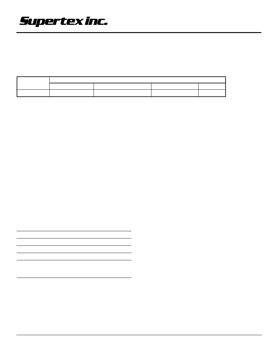
The Supertex HV5812 is a 20-channel serial input vacuum
fluorescent display driver. It combines a 20-bit CMOS shift regis-
ter, data latches, and control circuitry with high voltage MOSFET
outputs. The HV5812 is primarily designed for vacuum-fluores-
cent displays.
The CMOS shift register and latches allow direct interfacing with
microprocessor-based systems. Data input rates are typically
over 5.0MHz with 5V logic supply. Especially useful for inter-digit
blanking, the BLANKING input disables the output source drives
and turns on the sink drivers. Use with TTL may require external
pull-up resistors to ensure an input logic high.
Features
Operating voltage of to up to 80V
HVCMOS
technology for high performance
High speed source driver
Up to 3.3MHz data input rate
5.0V CMOS logic circuitry
Excellent noise immunity
Flexible high voltage supplies

2
HV5812
Symbol
Parameter
Min
Typ
Max
Units
Conditions
I
DSS
Output leakage current
-5.0
-15
µ
A
V
OUT
= 0V, T
A
= +70
∞
C
HV
OH
Output voltage
78
78.5
V
I
OUT
= -25mA, V
PP
= 80V
T
A
= +25
∞
C
HV
OH
Output Voltage
77
78
V
I
OUT
= -25mA, V
PP
= 80V
T
A
= +125
∞
C
HV
OL
Output Voltage
V
DD
= 5V
1.5
3.0
V
I
OUT
= 1.0mA, T
A
= +25
∞
C
HV
OL
Output Voltage
V
DD
= 5V
2.3
4.0
V
I
OUT
= 1.0mA, T
A
= +125
∞
C
I
SINK
Output pull-down current
V
DD
= 5V
2.0
3.5
mA
V
OUT
= 5.0V to V
PP
V
IH
Logic input voltage
V
DD
= 5V
3.5
5.3
V
V
IL
Logic input voltage
-0.3
0.8
V
I
IH
Logic input current
V
DD
= 5V
0.05
0.5
µ
A
V
IN
= V
DD
I
IL
Logic input current
V
DD
= 5V
-0.05
-0.5
µ
A
V
IN
= 0.8V
V
OH
Serial data out
V
DD
= 5V
4.5
4.7
V
I
OUT
= -200
µ
A
V
OL
Serial data out
V
DD
= 5V
200
250
mV
I
OUT
= 200
µ
A
f
CLK
Maximum clock frequency
V
DD
= 5V
8.0
MHz
T
J
= +25
∞
C
V
DD
= 5V
5.0
MHz
T
J
= +125
∞
C
I
DDQ
Supply current
V
DD
= 5V
100
300
µ
A
All outputs high
V
DD
= 5V
100
300
µ
A
All outputs low
I
PPQ
Supply current
10
100
µ
A
Outputs high, no Load
10
100
µ
A
Outputs low, no Load
Electrical Characteristics
DC Characteristics
(Over recommended operating conditions, T
A
= 25
∞
C, unless otherwise noted)
Symbol
Parameter
Min
Nom
Max
Units
V
DD
Supply voltage
4.5
5.5
V
V
PP
Supply voltage
20
80
V
T
J
Operating junction temperature
-40
+125
∞
C
Power-up sequence should be the following:
1. Connect ground.
2. Apply V
DD
.
3. Set all inputs (Data, CLK, etc.) to a known state.
4. Apply V
PP
.
5. The V
PP
should not drop below V
DD
or float during operation.
Power-down sequence should be the reverse of the above.
Recommended Operating Conditions

3
HV5812
Symbol
Parameter
Min
Typ
Max
Units
Conditions
t
PHL
Blanking to output delay
V
DD
= 5V
2000
ns
C
L
= 30pF, 50% to 50%
t
PLH
Blanking to output delay
V
DD
= 5V
1000
ns
C
L
= 30pF, 50% to 50%
t
f
Output fall time
V
DD
= 5V
1450
ns
C
L
= 30pF, 90% to 10%
t
r
Output rise time
V
DD
= 5V
650
ns
C
L
= 30pF, 10% to 90%
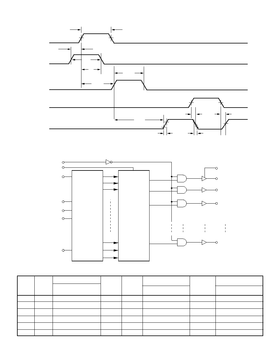
t
su
Data set-up time
75
ns
See timing diagram
t
h
Data hold time
75
ns
See timing diagram
t
pwd
Minimum data pulse width
150
ns
See timing diagram
t
pwclk
Minimum clock pulse width
150
ns
See timing diagram
t
cks
Minimum time between clock activation
300
ns
See timing diagram
and strobe
t
pws
Minimum strobe pulse width
100
ns
See timing diagram
t
sto
Typical time between strobe activation
500
ns
See timing diagram
and output transition
AC Characteristics
(T
A
= 25
∞
C, over operating conditions unless otherwise noted)
Input and Output Equivalent Circuits
V
DD
Input
GND
V
PP
L/T
GND
HV
OUT
Logic Inputs
GND
Data Out
Logic Data Output
High Voltage Outputs
V
DD

6
1235 Bordeaux Drive, Sunnyvale, CA 94089
TEL: (408) 744-0100 ∑ FAX: (408) 222-4895
www.supertex.com
11/12/01
©2001 Supertex Inc. All rights reserved. Unauthorized use or reproduction prohibited.