1
02/96/022
Supertex Inc. does not recommend the use of its products in life support applications and will not knowingly sell its products for use in such applications unless it receives an adequate "products liability
indemnification insurance agreement." Supertex does not assume responsibility for use of devices described and limits its liability to the replacement of devices determined to be defective due to
workmanship. No responsibility is assumed for possible omissions or inaccuracies. Circuitry and specifications are subject to change without notice. For the latest product specifications, refer to the
Supertex website: http://www.supertex.com. For complete liability information on all Supertex products, refer to the most current databook or to the Legal/Disclaimer page on the Supertex website.
32-Channel
±
40V Liquid Crystal Display Row Driver
Ordering Information
Features
Symmetrical
±
40V output swing
Active return to GND
15mA peak source/sink/GND current per channel
+5V control logic
Special shift register with clear
Phase shift control
Output enable
Data out enable
1MHz shift register
Surface mount package available
General Description
Not recommended for new designs.
The HV60 is a 32-channel liquid crystal display driver with 3-state
DMOS outputs. Each output can be set to +40V, -40V, or GND.
A symmetric waveform can be applied to a capacitive load using
the phase shift feature of the HV60.
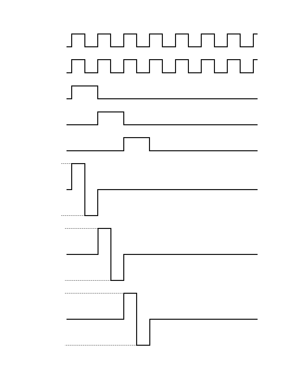
The HV60 consists of a 32-bit shift register with Clear, Enable, and
Phase Shift logic, and 32 high voltage output buffers. With the
Enable pin held low, all outputs are placed in the return to zero
(GND) state. When Enable is high, each output reflects the data
in its shift register bit. All outputs with a logic "0" in their shift
register will be in the return to zero state. Outputs with a logic "1"
in their shift register will reflect the state of the phase shift pin.
These outputs will be switched to V
PP
when phase shift is high and
V
NN
when phase shift is logic "0".
Additional functions provided are Shift Register Clear and Data
Out. All bits of the shift register are changed to logic "0" when Clear
is pulled low. With Clear at a logic "1", normal shift register
operation proceeds. The data output reflects the status of the
32nd shift register stage.
Absolute Maximum Ratings
Supply voltage, V
DD1
1
-6V
Supply voltage, V
DD2
1
+6V
Supply voltage, V
PP
1,2
+42V
Supply voltage, V
NN
1,2
-42V
Logic input levels
1
V
DD1
- 0.3V to V
DD2
+ 0.3V
Ground currrent
2
700mA
Continuous total power dissipation
3
1W
Operating temperature range
-40
∞
C to +85
∞
C
Storage temperature range
-65
∞
C to +150
∞
C
Notes:
1. All voltages are referenced to GND.
2. Duty cycle is limited by the total power dissipated in the package.
3. For operation above 25
∞
C ambient derate linearly to 85
∞
C at 16.7mW/
∞
C.
Package Options
Device
HV6008
HV6008PJ
HV6008DJ
HV6008PG
HV6008X
HV6008
44-J Lead Quad
44 -J Lead Quad
44-Lead Quad Plastic
Die
Plastic Chip Carrier
Ceramic Chip Carrier
Gullwing

2
HV6008
Symbol
Parameter
Min
Typ
Max
Units
Conditions
V
DD1
V
I
= 4V, V
DD1
= -6V
V
DD2
V
I
= 4V, V
DD2
= +6V
V
IH
Logic input high
+2
V
DD2
V
V
DD1
= -4.5V,
V
IL
Logic input low
V
DD1
-2
V
V
DD2
= +4.5V
V
OH
Logic output high
+2
V
V
OL
Logic output low
-2
V
I
IH
High-level logic input current
+3
µ
A
V
I
= V
DD
, V
DD1,2
= max
I
IL
Low-level logic input current
-50
µ
A
V
I
= 0V, V
DD1,2
= max
I
PP
High voltage supply current
+1
mA
Static, no load
I
NN
High voltage supply current
-1
mA
Static, no load
V
OH
Output voltage high
+39
V
V
CL
Output voltage clamp
-20
+20
mV
No load
V
OL
Output voltage low
-39
V
Z
OH
Output switch impedence high
1000
Z
CL
Output switch impedance clamp
500
Z
OL
Output switch impedance low
700
I
O
DC output current
Output H or L
5
mA
1 output only
Data out H or L
150
µ
A
Electrical Characteristics
(over recommended operating conditions unless noted)
DC Characteristics
I
DD1,2
V
DD
supply current
500
µ
A
AC Characteristics
Symbol
Parameter
Min
Typ
Max
Units
Conditions
t
WH
Width of high data pulse
500
ns
t
WL
Width of low data pulse
500
ns
t
SU
Data set-up time before clock falls
25
ns
t
H
Data hold time after clock falls
10
ns
Phase shift duty cycle
50
%
Recommended Operating Conditions
V
PP
, V
NN
=
±
40
V
PP
, V
NN
=
±
40
I
O
=
±
15mA
V
DD1
= -4.5V
V
DD2
= +4.5V
I
OH
= -15
µ
A
I
OL
= 250
µ
A
Symbol
Parameter
Min
Typ
Max
Units
V
DD1
Logic supply voltage
-4
-6
V
V
DD2
Logic supply voltage
+4
+6
V
V
PP
High voltage supply
+10
+40
V
V
NN
High voltage supply
-10
-40
V
V
IH
High-level input voltage
+2V
V
DD2
V
V
IL
Low-level input voltage
-2V
V
DD1
V
I
O Pk.
Peak output current (any state)
±
80
mA
T
A
Operating free-air temperature
-40
+70
∞
C
f
DIN
Input data rate
1
MHz
f
PS
Phase shift rate
20
KHz
Note:
Power-up sequence should be the following:
1. Connect ground.
3.
Set all inputs (Data, CLK, Enable, etc.) to a known state.
2. Apply V
DD
.
4.
Apply V
PP
and V
NN
.
Power-down sequence should be the reverse of the above.
5
1235 Bordeaux Drive, Sunnyvale, CA 94089
TEL: (408) 744-0100 ∑ FAX: (408) 222-4895
www.supertex.com
02/06//02
©2002 Supertex Inc. All rights reserved. Unauthorized use or reproduction prohibited.
HV6008
21
6
40
41
42
43
44
1
2
3
4
5
39 38 37 36 35 34
33
32
31
30
29
18
22
20
19
7
8
9
10
11
12 13 14 15 16 17
28
27
26
25
24
23
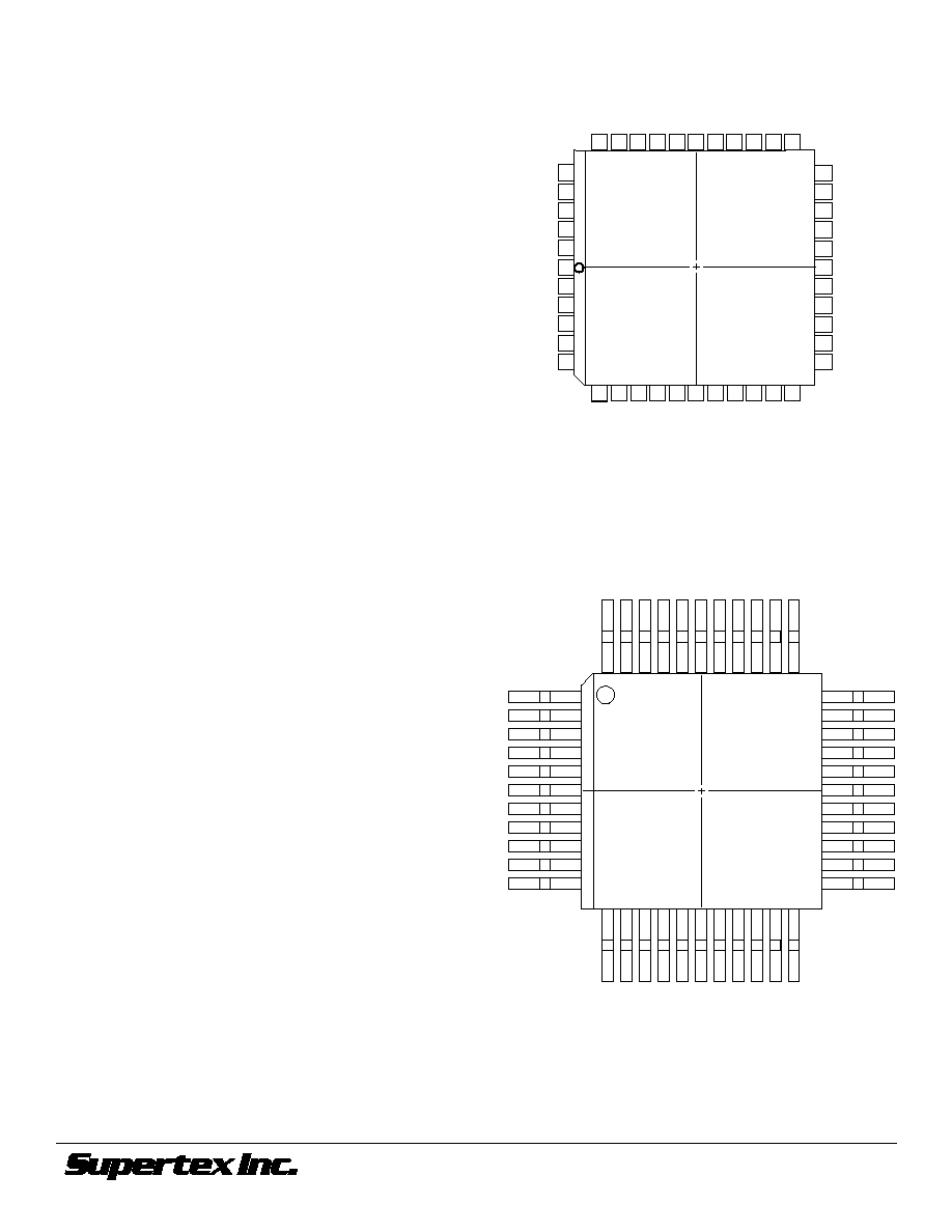
44-Pin J-Lead
Pin
Function
1
HV
OUT
16
2
HV
OUT
15
3
HV
OUT
14
4
HV
OUT
13
5
HV
OUT
12
6
HV
OUT
11
7
HV
OUT
10
8
V
PP
9
HV
OUT
9
10
HV
OUT
8
11
HV
OUT
7
12
HV
OUT
6
13
HV
OUT
5
14
HV
OUT
4
15
HV
OUT
3
16
HV
OUT
2
17
HV
OUT
1
18
Data In
19
GND
20
Phase Shift
21
Clock
22
Clear
Pin
Function
23
V
DD 1
24
Enable
25
V
DD
2
26
GND
27
Data Out
28
HV
OUT
32
29
HV
OUT
31
30
HV
OU
30
31
HV
OUT
29
32
HV
OUT
28
33
HV
OUT
27
34
HV
OUT
26
35
HV
OUT
25
36
HV
OUT
24
37
V
NN
38
HV
OUT
23
39
HV
OUT
22
40
HV
OUT
21
41
HV
OUT
20
42
HV
OUT
19
43
HV
OUT
18
44
HV
OUT
17
Pin Configurations
Package Outlines
44-Pin Quad Palstic Package
Pin
Function
1
HV
OUT
21
2
HV
OUT
20
3
HV
OUT
19
4
HV
OUT
18
5
HV
OUT
17
6
HV
OUT
16
7
HV
OUT
15
8
HV
OUT
14
9
HV
OUT
13
10
HV
OUT
12
11
HV
OUT
11
12
HV
OUT
10
13
V
PP
14
HV
OUT
9
15
HV
OUT
8
16
HV
OUT
7
17
HV
OUT
6
18
HV
OUT
5
19
HV
OUT
4
20
HV
OUT
3
21
HV
OUT
2
22
HV
OUT
1
Pin
Function
23
Data In
24
GND
25
Phase Shift
26
Clock
27
Clear
28
V
DD1
29
Enable
30
V
DD2
31
GND
32
Data Out
33
HV
OUT
32
34
HV
OUT
31
35
HV
OUT
30
36
HV
OUT
29
37
HV
OUT
28
38
HV
OUT
27
39
HV
OUT
26
40
HV
OUT
25
41
HV
OUT
24
42
V
NN
43
HV
OUT
23
44
HV
OUT
22
44-pin J Lead Package
6
40
41
42
43
44
1
2
3
4
5
39 38 37 36 35 34 33 32 31 30 29
18
28
27
26
25
24
23
22
21
20
19
7
8
9
10 11 12 13 14 15 16 17
top view
top view
44-pin Quad Plastic Gullwing Package