 | –≠–ª–µ–∫—Ç—Ä–æ–Ω–Ω—ã–π –∫–æ–º–ø–æ–Ω–µ–Ω—Ç: HV623 | –°–∫–∞—á–∞—Ç—å:  PDF PDF  ZIP ZIP |
12-122
HV623
32-Channel 128-Level Amplitude Gray-Shade
Display Column Driver
Absolute Maximum Ratings
Supply voltage, V
DD
1
-0.5V to +7.5V
Supply voltage, V
PP
1
-0.5V to +90V
Logic input levels
1
-0.5 to V
DD
+ 0.5V
Ground current
2
1.5A
Continuous total power dissipation
3
1W
Operating temperature range
-40
∞
C to +70
∞
C
Storage temperature range
-65
∞
C to +150
∞
C
Lead temperature 1.6mm (1/16 inch)
260
∞
C
from case for 10 seconds
Notes:
1. All voltages are referenced to GND.
2. Duty cycle is limited by the total power dissipated in the package.
3. For operation above 25
∞
C ambient derate linearly to 70
∞
C at 22.2mW/
∞
C.
Features
5V CMOS inputs
Up to 80V modulation voltage
Capable of 128 levels of gray shading
20MHz data throughput rate
32 outputs per device (can be cascaded)
Pin-programmable shift direction (DIR)
D/A conversion cycle time is 32
µ
s
Diodes in output structure allow usage
in energy recovery systems
Integrated HVCMOS
Æ
technology
Available in 3-sided 64-lead gullwing package
General Description
The HV623 is a 32-channel driver IC for gray shade display use.
It is designed to produce varying output voltages between 3 and
80 volts. This amplitude modulation at the output is facilitated by
an external ramp voltage V
R
. See Theory of Operation for detailed
explanation.
This device consists of a dual 16-bit shift registers, 32 data latches
and comparators, and control logic to preform 128 levels of gray
shading. There are 7 bits of data inputs. Data is shifted through the
shift registers at both edges of the clock, resulting a data transfer
rate of twice of the shift clock frequency. When the DIR pin is high,
CSI/CSO is the input/output for the chip select pulse. When DIR
is low, CSI/CSO is the output/input for the chip select pulse. The
DIR = HIGH also allows the HV623 to shift data in the counter-
clockwise direction when viewed from the top of the package.
When the DIR pin is low, data is shifted in the clockwise direction.
The output circuitry allows the energy which is stored in the output
capacitance to be returned to V
PP
through the body diode of the
output transistor.
Ordering Information
Package Option
Device
64-Lead 3-sided Plastic Gullwing
HV623
HV623PG
12-123
HV623
Symbol
Parameter
Min
Typ
Max
Units
Conditions
I
AOH
High-voltage analog output source current
See Performance Curves
mA
V
PP
= 80V
See test circuit
I
AOL
High-voltage analog output sink current
See Performance Curves
mA
V
PP
= 80V, V
DD
= 4.5V
V
AO
= 2V
V
O
Maximum delta voltage between high voltage outputs
±
0.2
V
At all gray levels
of the same level
Symbol
Parameter
Min
Typ
1
Max
Units
Conditions
I
DD
V
DD
supply current
12
20
mA
f
SC
= 10MHz
f
CC
= 8MHz
I
DDQ
Quiescent V
DD
supply current
100
µ
A
All V
IN
= 0V, V
DD
= max
I
IH
High-level input current
1.0
50
µ
A
V
IH
= V
DD
I
IL
Low-level input current
-1.0
-50
µ
A
V
IL
= 0V
C
IN
2
Input capacitance (data, LC, SC, CC)
15
pF
V
IN
= 0V, f = 1MHz
I
OH
High-level output current
-2
mA
V
DD
= 4.5V
I
OL
Low-level output current
2
mA
V
DD
= 4.5V
Notes
1. All typical values are at V
DD
= 5.0V.
2. Guaranteed by design.
Electrical Characteristics
(at T
A
= 25
∞
C, over operating conditions unless otherwise specified)
Low-Voltage DC Characteristics (Digital)
Symbol
Parameter
Min
Typ
Max
Units
Conditions
I
PP
V
PP
supply current for bias circuit
2
mA
Depending on external
bias circuit, see Table 1.
High-Voltage Bias Circuit for Output Variation Control
High-Voltage DC Characteristics
Symbol
Parameter
Min
Typ
Max
Units
Conditions
I
DD
V
DD
supply current
100
µ
A
f
SC
=10MHz
f
CC
= 8MHz
I
DDQ
Quiescent V
DD
supply current
100
µ
A
All V
IN
= 0V, V
DD
= max
Low-Voltage DC Characteristics (Analog)
Symbol
Parameter
Min
Typ
Max
Units
V
DD
Low-voltage digital supply voltage
4.5
5.0
5.5
V
V
DD
Low-voltage analog supply voltage
4.5
5.0
5.5
V
V
IH
High-level input voltage (analog and digital)
V
DD
-1
V
DD
V
V
IL
Low-level input voltage (analog and digital)
0
1
V
V
BIAS
I
PP
control circuit bias voltage
-2
0
V
V
CTL
I
PP
control circuit control voltage
0
2
V
V
PP
High-voltage supply
-0.3
80
V
V
R
Ramp voltage
0
V
PP
-2
V
f
SC
Shift clock operating frequency (at V
DD
= 5.5V)
10.2
MHz
T
A
Operating free-air temperature
-40
70
∞
C
Recommended Operating Conditions
Notes:
Power-up sequence should be the following:
1. Connect ground. 2. Apply V
DD
. 3. Set all inputs (Data, CLK, Enable, etc.) to a known state. 4. Apply V
PP
.
Power-down sequence should be the reverse of the above.
12-124
HV623
Option 1
Option 2
V
BIAS
V
CTL
R
CTL
I
PP
V
BIAS
V
CTL
R
CTL
I
PP
(V)
(V)
(
)
(mA)
(V)
(V)
(
)
(mA)
0
0.1
56K
2
-1.0
0
56K
4
0
1.0
56K
7
-2.0
0
56K
5.5
Symbol
Parameter
Min
Typ
Max
Units
Conditions
f
SC
Shift clock operating frequency
10.2
MHz
f
DIN
Data-in frequency
20.4
MHz
t
SS
CSI/CSO pulse to shift clock setup time
40
ns
t
HS
CSI/CSO pulse to shift clock hold time
0
ns
t
WA
CSI pulse width
49
ns
t
DS
Data to shift clock setup time
20
ns
t
DH
Data to shift clock hold time
0
ns
t
WD
Data-in pulse width
24
ns
t
WLC
Load count pulse width
98
ns
t
DLCR
Load count to ramp delay
1
µ
s
t
DRCC
1
Ramp to count clock delay
0.47
µ
s
t
DSL
Shift clock to load count delay time
98
ns
t
CSC
Shift clock cycle time
98
ns
t
WSC
Shift clock pulse width
49
ns
t
CCC
Count clock cycle time
98
ns
t
WCC
Count clock pulse width
49
ns
Note 1: Count clock starts counting after 0.47
µ
s min. This is equivalent to a time duration for a linear ramp V
R
to ramp from 0 to 3V, assuming the minimum value of T
RR
,
ramp size time of 12
µ
s for V
R
= 80V.
AC Characteristics
(V
DD
= 5.5V, T
A
= 25
∞
C)
Logic Timing
Electrical Characteristics
V
RAMP
Timing
Note 2: The maximum ramp hold time may be longer than 15
µ
s, but the output voltage HV
OUT
will droop due to leakage.
Table 1:
Schemes to control I
PP
bias current, typical I
PP
Symbol
Parameter
Min
Typ
Max
Units
Conditions
t
CR
Cycle time of ramp signal
15
µ
s
t
RR
Ramp rise time
12
µ
s
t
HR
2
Ramp hold time
2
15
µ
s
t
FR
Ramp fall time
TBD
3
µ
s
HV623
VCTL
VCTL
RCTL
RCTL
VBIAS
-
+
-
+
12-125
Pin #
Name
Function
30-36
D1-D7
Inputs for binary-format parallel data.
26
SC (Shift Clock)
Triggers data on both rising and falling edges. This implies that the data rate is always twice the clock
rate (data rate = 20MHz max if clock rate = 10MHz max).
22
CSI (Chip
Input pin for the chip select pulse (when DIR is high).
Select Input)
Output pin for the chip select pulse (when DIR is low).
43
CSO (Chip
Input pin for the chip select pulse (when DIR is low).
Select Output)
Output pin for the chip select pulse (when DIR is high).
40
LC
Input for a pulse whose rising edge causes data from the input latches to enter the comparator latches,
(Load Count)
and whose falling edge initiates the conversion of this binary data to an output level (D-to-A).
Also, the HV
OUT
will clear to zero after the load count is initiated.
42
CC (Count Clock) Input to the count clock generator whose increments are compared to the data in the comparator latches.
18, 47
V
R
High-voltage ramp input for charging the output stage hold capacitors (C
H
).
This input can be linear or non-linear as desired.
28
DIR
When this pin is connected to V
DD
, input data is shifted in ascending order,
i.e., corresponding to HV
OUT
1 to HV
OUT
32. When connected to LVGND, input data is shifted
in descending order, i.e., corresponding to HV
OUT
32 to HV
OUT
1.
27, 38
LVGND
This is ground for the logic section.
HVGND and LVGND should be connected together externally.
17, 48
HVGND
This is ground for the high-voltage (output) section.
HVGND and LVGND should be connected together externally.
19, 45
V
PP
This input biases the output source followers.
1-16
HV
OUT
1-
High-voltage outputs.
49-64
HV
OUT
32
21
V
DD
(Analog)
Low-voltage analog supply voltage.
29
V
DD
(Digital)
Low-voltage digital supply voltage.
24
V
CTL
Voltage supply pin to prevent output voltage from being affected by its adjacent outputs (V
CTL
= 2V for a
particular panel). The combination of V
CTL
and R
CTL
will reduce the output voltage variation to less than
±
0.2V of delta voltage between high voltage outputs of the same level at all gray levels.
25
R
CTL
Current sense resistor to ground to prevent output voltage from being affected by its adjacent outputs
(R
CTL
= 56K
for a particular panel). See V
CTL
function above.
Pin Definitions
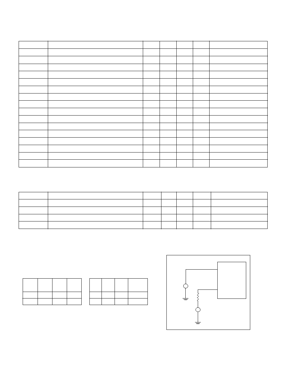
Input and Output Equivalent Circuits
V
DD
Input
GND
(Logic)
Logic Inputs
GND
(Logic)
Data Out
Logic Data Output
V
DD
HV623
12-126
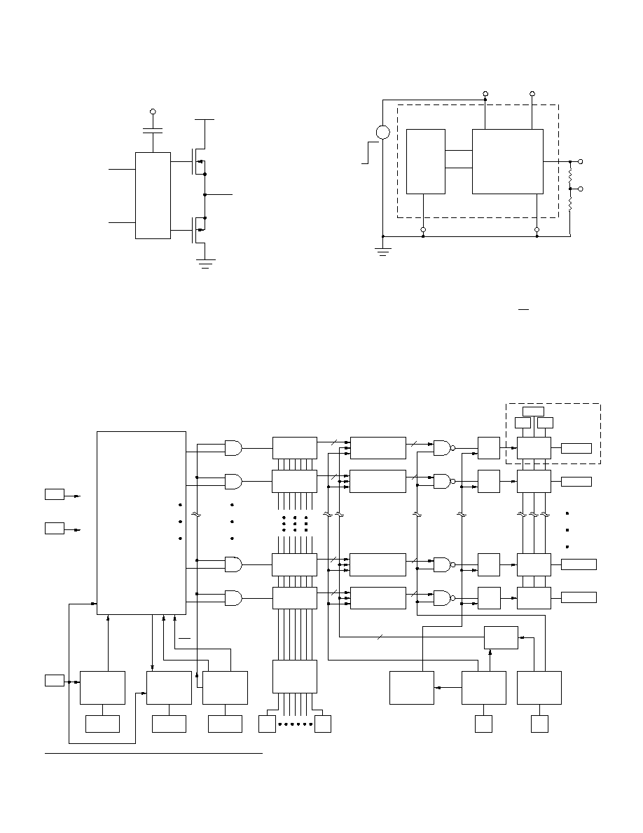
Functional Block Diagram
Output
Stage
Latches and
Comparators
Latches and
Comparators
Latches and
Comparators
Latches and
Comparators
Load
Count
CC
Clear
Dual
16-bit
Shift Registers
V
R
GND
V
PP
HV
OUT
1
Output
Stage
HV
OUT
2
Data In
Buffers
HV
OUT
31
V
CTL
R
CTL
Output
Stage
Counter
Reset
Counter
HV
OUT
32
Data
Latches
Data
Latches
Data
Latches
Data
Latches
RS
F/F
RS
F/F
RS
F/F
RS
F/F
7
7
7
7
7
7
7
7
7
L/E
L/E
L/E
L/E
Clear
Pulse
Generator
Load
Count
Buffer
Count
Clock
Buffer
SC
Load
Count
SC
SC
Shift
Clock
Buffer
CSI
I/O
Buffers
CC
LC
D1
D7
DIR
CSO
I/O
Buffers
See Output Stage Detail
Output
Stage
1
2
31
32
SC = Shift Clock
LC = Load Count
CC = Count Clock
CSI = Chip Select Input
CSO = Chip Select Output
*Strobe = twice the SC frequency
Logic
70V
HV623
0V
Output
Stage
V
R
HVGND
LVGND
V
PP
= 80V
+
≠
HV
OUT
1K
V
tst
10K
+
-
1. Set HV
OUT
= Low.
2. Apply V
PP
= 80V.
3. Apply a step voltage of 70V at V
R
(slew rate = 4.1V/
µ
s).
4. Measure voltage across the 1K
resistor.
5. Output source current can be calculated by using
V
tst
.
1K
Internal
Logic
&
Bias
Circuit
V
CTL
R
CTL
V
R
V
PP
C
H
Q
1
Q
2
HV
OUT
Test Circuit
High-voltage Analog Output Source Current (I
AOH
)
For gray shade #1 (000 0000)
Output Stage Detail
HV623

12-127
HV623
Gray Scale Voltage
Gray Shade Decoding Scheme
Shade Number
D7
D6
D5
D4
D3
D2
D1
128
1
1
1
1
1
1
1
127
1
1
1
1
1
1
0
126
1
1
1
1
1
0
1
125
1
1
1
1
1
0
0
124
1
1
1
1
0
1
1
123
1
1
1
1
0
1
0
122
1
1
1
1
0
0
1
121
1
1
1
1
0
0
0
7
0
0
0
0
1
1
0
6
0
0
0
0
1
0
1
5
0
0
0
0
1
0
0
4
0
0
0
0
0
1
1
3
0
0
0
0
0
1
0
2
0
0
0
0
0
0
1
1
0
0
0
0
0
0
0
0
V
R
HV
OUT
HV
OUT
HV
OUT
HV
OUT
HV
OUT
1 2
∑ ∑ ∑
127
Gray Scale Voltage
Clock Cycle
(000 0000)
(111 1111)
Typical Panel Connections
1
32
1
32
1
32
32
1
32
1
32
1
V
R
, V
PP
LVGND, HVGND,
SC, LC, CC, CSO
V
R
, V
PP
LVGND, HVGND,
SC, LC, CC, CSI
Data Bus
(7)
DIR = LOW
DIR = HIGH
Data Bus
(7)
Display Panel
(Example)
12-128
HV623
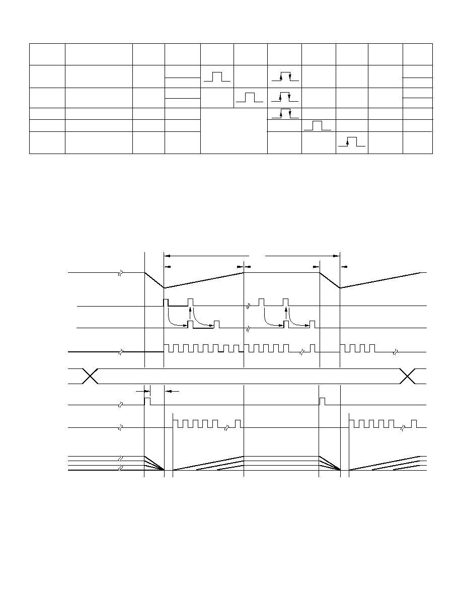
Sequence
Function
DIR
Data-In
CSI
CSO
Shift
Load
Count
V
R
HV
OUT
(D1 - D7)
Clock
Count
Clock
1
Shift Data
H
H
Output
L
L
L
L
from HV
OUT
1 to 32
L
H
2
Shift Data
L
H
Output
L
L
L
L
from HV
OUT
32 to 1
L
H
3
Load Shift Register
X
X
L
L
L
-
4
Load Counter
X
X
Pre-define by 1 or 2
L
L
L
-
5
Counting/Voltage
X
X
L
L
Initiates
-
Conversion
V
RAMP
Function Table
Chip Select
Input (CSI)
Load
First
Device
Load
Second
Device
Load
Last
Device
1
2
3
4
5
128
t
RR
t
FR
t
DLCR
V
R
Chip Select
Output (CSO)
Shift Clock
(SC)
Load Count*
(LC)
Count Clock
(CC)
OUT
HV
Data from Data Bus (See Detailed Timing)
t
CR
t
HR
*HV
OUT
will clear to zero with load count.
1
2
3
4
5
128
Data In
(D1 - D7)
Timing Diagrams
(a) Basic System Timing

12-129
HV623
(b) Detailed Device Timing
t
WA
t
SS
t
HS
DATA
SET 1
DATA
SET 2
DATA
SET 3
DATA
SET 31
DATA
SET 32
t
DS
t
DH
t
WD
t
WLC
DSL
t
DATA
SET 1
DATA
SET 31
LOADING LAST DEVICE
NEXT LOADING CYCLE
Chip Select
Input (CSI)
Data
(D1-D7)
Shift Clock
(SC)
Load Count
(LC)
Count Clock
(CC)
R
V
Count
Clock 1
Count
Clock 128
0V
3V
DLCR
t
DRCC
t
80V
t
CSC
SC 2
SC 16
SC 1
SC 16
WCC
t
CCC
t
SC 1
Typical Performance Curves
Sink Output Characteristics
Source Output Characteristics
V
GS
Volts
V
GS
Volts
I
O
(milliamperes)
I
O
(milliamperes)
0
2
1
4
3
5
6
7
8
0
2
1
4
3
5
6
7
8
15
12
9
6
3
0
15
12
9
6
3
1

12-130
HV623
Pin
Function
64-Pin PG Package
Pin
Function
1
HV
OUT
1
2
HV
OUT
2
3
HV
OUT
3
4
HV
OUT
4
5
HV
OUT
5
6
HV
OUT
6
7
HV
OUT
7
8
HV
OUT
8
9
HV
OUT
9
10
HV
OUT
10
11
HV
OUT
11
12
HV
OUT
12
13
HV
OUT
13
14
HV
OUT
14
15
HV
OUT
15
16
HV
OUT
16
17
HVGND
18
V
R
19
V
PP
20
N/C
21
V
DD
(Analog)*
22
CSI
Pin Configuration
Pin
Function
23
N/C
24
V
CTL
25
R
CTL
26
SC (Shift Clock)
27
LVGND
28
DIR
29
V
DD
(Digital)*
30
D
7
31
D
6
32
D
5
33
D
4
34
D
3
35
D
2
36
D
1
37
N/C
38
LVGND
39
N/C
40
LC (Load Count)
41
N/C
42
CC (Count Clock)
43
CSO
44
N/C
45
V
PP
46
N/C
47
V
R
48
HVGND
49
HV
OUT
17
50
HV
OUT
18
51
HV
OUT
19
52
HV
OUT
20
53
HV
OUT
21
54
HV
OUT
22
55
HV
OUT
23
56
HV
OUT
24
57
HV
OUT
25
58
HV
OUT
26
59
HV
OUT
27
60
HV
OUT
28
61
HV
OUT
29
62
HV
OUT
30
63
HV
OUT
31
64
HV
OUT
32
Package Outlines
* Analog V
DD
and digital V
DD
may be connected
separately for better noise immunity.
3-Sided Plastic QFP 64-pin Gullwing Package
top view
Index
1
24
64
41
25
40
Theory of Operation
The HV623 has two primary functions:
1) Loading data from the data bus and,
2) Gray-shade conversion
(converting latched data to output voltages).
Since the device was developed initially for flat panel displays, the
operation will be described in terms that pertain to that technol-
ogy. As shown by the Typical Drive Scheme, several HV623
packages are mounted at the top and bottom of a display panel.
Data exists on a 7-bit bus (adjacent PC board traces) at top and
bottom. The D1 through D7 inputs of each chip take data from the
bus when either a CSI or CSO pulse is present at the chip. These
pulses therefore act as a combination CHIP SELECT and LOCA-
TION STROBE. Because of the way the chip HV
OUT
pins are
sequenced, data on the bus at the bottom of the display panel will
be entered into the left-most chip as HV
OUT
1
,
HV
OUT
2
,
etc. up to
HV
OUT
32. The CSI pulse will accomplish this with DIR = High.
Loading Data from Data Bus
Here is the full data-entry sequence:
1) The microcontroller puts data on the bus (7 bits)
2) To enter the data into the 32 sets of 7 latches on the first chip,
the shift clock rises. This positive transition is combined with
the CSI pulse and is generated only once to strobe the data into
the first set of latches. (These latches eventually send data to
the HV
OUT
1). The data on the bus then changes, the shift clock
falls, and this negative transition is combined with the CSI
pulse, which is now propagated internally, to strobe the new
data into the next set of 7 latches (which will end up as
HV
OUT
2). This internal CSI pulse therefore runs at twice the
shift clock rate.
3) When the last set of 7 latches in the first chip has been loaded
(HV
OUT
32), the CSI pulse leaves chip 1 and enters chip 2. The
exit pin is called CSO and the chip 2 entry pin is CSI . For chips
at the top of the panel things are reversed: DIR is low, entry pins
are CSO and exit pins are CSI , because the data-into-latches
sequence is in descending order, HV
OUT
32 down to HV
OUT
1.
4) The buses may of course be separate, and data can be strobed
in on an interleaved basis, etc., but those complications will be
left to systems designers.

12-131
HV623
When data has been loaded into all 32 outputs of all chips (top and
bottom of the display panel), the load count pin is pulsed. On its
rising transition, all output levels are reset to zero and all the data
in the input latches is transferred to a like number of comparator
latches, (thus leaving the data latches ready to receive new data
during the following operations). After the transfer, the load count
pin is brought low. This transition begins the events that convert
the binary data into a gray-shade level.
Gray-shade Conversion
1) The COUNT CLOCK is started. An external signal is applied
to the COUNT CLOCK pin, causing the counter on each chip
to increment from binary 000 0000 to 111 1111 (0 to 127).
2) At the same time, the V
R
voltage is applied to all chips, via
charging transistors, causing the HOLD CAPACITOR (C
H
) on
each output to experience a rise in voltage.
3) The logic control compares the count in the comparator latch
to the count clock. The gate voltage of Q
1
and the output
voltage HV
OUT
will ramp up at the same rate as V
R
.
4) Once V
R
has reached the maximum voltage, then all the pixels
will be at the final value. (See Output Gray Scale Voltage.)
Output Voltage Variation
The output voltage of the HV623 is determined by the logic and
the ramp voltage V
R
. It is possible that the output voltage may be
coupled to an unacceptable level due to its adjacent outputs
through the panel. In order to solve this problem, internal logic
(refer to Output Stage Detail) is integrated in the IC to minimize
the effect.
Two external pins V
CTL
and R
CTL
allow the feasibility to control the
current flowing through Q
2
. The V
CTL
pin is connected to a voltage
source and the R
CTL
pin is connected to ground through a resistor
(2V and 56K
are used for a particular panel). The internal bias
circuit will drive the resistor to a voltage level that is equal to the
V
CTL
voltage at steady state through an operational amplifier. The
current flowing through Q1 and Q2 will be limited to V
CTRL
/R
CTRL
.
This combination of V
CTL
and R
CTL
will reduce the output voltage
variation to less than
±
0.2V of delta voltage for each gray shade,
independent of its adjacent output voltages.