 | –≠–ª–µ–∫—Ç—Ä–æ–Ω–Ω—ã–π –∫–æ–º–ø–æ–Ω–µ–Ω—Ç: HV732 | –°–∫–∞—á–∞—Ç—å:  PDF PDF  ZIP ZIP |
Supertex inc.
Supertex inc.
∑
1235 Bordeaux Drive, Sunnyvale, CA 94089
∑
Tel: (408) 222-8888
∑
FAX: (408) 222-4895
∑
www.supertex.com
1
NR040506
HV732
Initial Release
High Speed ±100V 2A
Integrated Ultrasound Pulser
Features
HVCMOS technology for high performance
0 to ±100V output voltage
±2A source and sink current
Built-in damping for RTZ waveform capability
Gate-clamp for quick output amplitude ramping
Up to 40MHz operation frequency
±3ns matched delay times
Second harmonic is less than -40dB
1.8V to 3.3V CMOS logic interface
7x7 thermally-enhanced 44-lead QFN MCM
Application
Medical ultrasound imaging
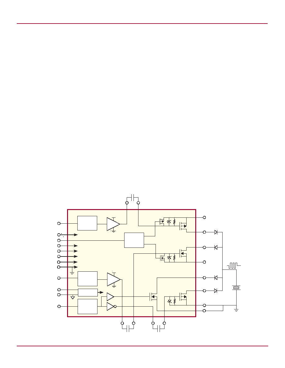
General Description
The Supertex HV732 is a single, complete, high-voltage,
high-speed, ultrasound transmitter pulser. It is designed for
medical ultrasound imaging applications.
The HV732 has built-in damping for faster RTZ waveform
capability and high voltage MOSFET gate-clamping function
for quick ramping of the output voltage amplitude.
The HV732 consists of a control logic circuit, level translators,
MOSFET gate drive buffers, clamp circuits, and high current,
high voltage MOSFETs as the ultrasound transmitter pulser
output stage.
In the output stage there are two pairs of MOSFETs. Each
pair consists of a P-channel and an N-channel MOSFET.
They are designed to have the same impedance, and can
provide peak currents of over ±2 amps. The built-in MOSFET
gate driver outputs swing 0 to 12V on P
DR
and N
DR
pins. The
P-channel damp output swings 0 to ≠5V on the DMPO pin.
Typical Application Circuit
Level
Trans.
DAMP
Level
Trans.
+12V
Level
Trans.
+12V
V
SUB
Substrate, PAD
1
+5 to 12V
V
DD
AGND
V
LL
V
LN
CLAMP
EN
GND
+1.8 to 3.3V
-5V
on/off
Clamp
Circuit
N
IN
AV
DD
Bias
P
IN
P
DR
TX
N
V
NN
TX
P
V
PP
OUT
N
OUT
P
RGND
P
DMPI
N
DR
DMPO
N
GATE
P
GATE
10nF
0 to +100V
0 to -100V
HV
OUT
PAD
3
PAD
2
0V
RGND
N
10nF
10nF
Buffer
Buffer

2
NR040506
HV732
Ordering Information
Device
Package Options
44-Lead QFN
HV732
HV732K6
HV732K6-G
-G indicates package is RoHS compliant (`Green')
Absolute Maximum Ratings
Parameter
Value
V
LL
, logic supply
-0.5V to +5.5V
V
DD
, positive gate drive supply
-0.5V to +15V
AV
DD
, positive gate drive supply
-0.5V to +15V
V
LN
, Negative gate drive supply
-5.5V to +0.5V
V
PP
-V
NN
, differential high voltage supply
+220V
V
PP
, high voltage positive supply
-0.5V to +200V
V
NN
, high voltage negative supply
+0.5V to -200V
Storage temperature
-65∞C to 150∞C
Thermal enhanced package power
dissipation
1.5W
Symbol
Parameter
Min
Typ
Max
Units
Conditions
Operating Supply Voltages and Current
(Over recommended operating conditions unless otherwise specifi ed: AV
DD
= V
DD
= 12V, V
LL
= 3.3V, V
LN
= -5V, T
A
= 25∞C)
Absolute Maximum Ratings are those values beyond which damage to the device may
occur. Functional operation under these conditions is not implied. Continuous operation
of the device at the absolute rating level may affect device reliability. All voltages are
referenced to device ground.
Power-Up Sequence
1
V
PP
and V
SUB
2
V
NN
3
V
LN
4
V
DD
5
V
LL
V
LL
Logic supply
1.8
3.3
3.6
V
---
AV
DD
Positive analog supply
9.0
-
12.6
V
---
V
DD
Positive drive supply
9.0
-
12.6
V
---
V
PP
High voltage positive supply for HV
OUT
P1
0
-
100
V
---
V
NN
High voltage negative supply for HV
OUT
N1
-100
-
0
V
---
V
LN
High voltage negative supply for HV
OUT
N2
-4.75
-5.0
-5.25
V
---
V
SUB
High voltage positive supply for to bias
substrate
-
-
100
V
Need to be the most positive supply on the
device
I
DDQ
V
DD
current EN = Low
-
175
290
A
---
I
DDEN
V
DD
current EN = High
-
1.7
2.8
mA
P
IN
= N
IN
= Low
I
DDEN
V
DD
current at 5MHz PW
-
7.5
-
mA
f = 5.0MHz, PW D% = 1.0%
No cap on P
DR
, N
DR
I
PPQ
V
DD
current EN = Low
-
2.0
5.0
A
V
PP
= +100V, V
NN
= -100V
I
PPEN
V
DD
current EN = High
-
140
180
A
P
IN
= N
IN
= Low, V
PP
= +100V, V
NN
= -100V
I
NNQ
V
DD
current EN = Low
-
-1.0
-3.0
A
V
PP
= +100V, V
NN
= -100V

3
NR040506
HV732
I
NNEN
V
DD
current EN = High
-
-140
-180
A
P
IN
= N
IN
= Low, V
PP
= +100V, V
NN
= -100V
I
LLQ
V
DD
current EN = Low
-
1.0
5.0
A
---
I
LLEN
V
DD
current EN = High
-
16
25
A
P
IN
= N
IN
= Low
I
LNQ
V
DD
current EN = Low
-
-1.0
-5.0
A
---
I
LNEN
V
DD
current EN = High
-
-230
-320
A
P
IN
= N
IN
= Low
Operating Supply Voltages and Current (cont.)
(Over recommended operating conditions unless otherwise specifi ed: AV
DD
= V
DD
= 12V, V
LL
= 3.3V, V
LN
= -5V, T
A
= 25∞C)
Symbol
Parameter
Min
Typ
Max
Units
Conditions
DC Electrical Characteristics
(Over recommended operating conditions unless otherwise specifi ed: AV
DD
= V
DD
= 12V, V
LL
= 3.3V, V
LN
= -5V, T
A
= 25∞C)
Symbol
Parameter
Min
Typ
Max
Units
Conditions
Output P-Channel MOSFET, TX
P
I
OUT
Output saturation current
-2.0
-
-
A
V
GS
= -10V, V
DS
= -25V
R
ON
Channel resistance
-
-
8
V
GS
= -10V, I
DS
= -1.0A
R
GS
Gate to source resistor
10
-
50
K
I
GS
= -100A
V
GS
Source to gate zener voltage
-13.2
-
-25
V
I
GS
= -2.0A
V
GSF
Gate zener forward voltage
-0.5
-
-0.8
V
---
V
GS(th)
Gate threshold voltage
-1.0
-
-2.4
V
I
DS
= -1.0mA
C
ISS
Input capacitance
-
-
200
pF
V
GS
= 0V, V
DS
= -25V, f = 1Mhz
C
OSS
Output capacitance
-
25
55
pF
Output N-Channel MOSFET, TX
N
I
OUT
Output saturation current
2.0
-
-
A
V
GS
= -10V, V
DS
= -25V
R
ON
Channel resistance
-
7.0
V
GS
= -10V, I
DS
= -1.0A
R
GS
Gate to source resistor
10
-
50
K
I
GS
= -100A
V
GS
Source to gate zener voltage
13.2
-
25
V
I
GS
= -2.0A
V
GSF
Gate zener forward voltage
0.5
-
0.8
V
---
V
GS(th)
Gate threshold voltage
1.0
-
2.0
V
I
DS
= -1.0mA
C
ISS
Input capacitance
-
-
110
pF
V
GS
= 0V, V
DS
= -25V, f = 1Mhz
C
OSS
Output capacitance
-
28
60
pF
Symbol
Parameter
Min
Typ
Max
Units
Conditions
Output P-Channel Damp MOSFET, OUT
P
I
OUT
Output saturation current
-
-1.0
-
A
V
GS
= -10V, V
DS
= -25V
R
ON
Channel resistance
-
-
30
V
GS
= -10V, I
DS
= -1.0A
R
GS
Gate to source resistor
-
75
100
K
I
GS
= -100A
V
GS
Source to gate zener voltage
-13.2
-
-25
V
I
GS
= -2.0A
V
GSF
Gate zener forward voltage
0.5
-
0.8
V
---
V
GS(th)
Gate threshold voltage
-1.0
-
-2.6
V
I
DS
= -1.0mA
C
ISS
Input capacitance
-
-
200
pF
V
GS
= 0V, V
DS
= -25V, f = 1Mhz
C
OSS
Output capacitance
-
-
60
pF
Symbol
Parameter
Min
Typ
Max
Units
Conditions
4
NR040506
HV732
Output N-Channel Damp MOSFET, OUT
N
I
OUT
Output saturation current
1.0
-
-
A
V
GS
= 10V, V
DS
= 25V
R
ON
Channel resistance
-
-
22
V
GS
= 10V, I
DS
= 0.5A
V
GS
Source to gate zener voltage
1.0
-
2.6
V
I
DS
= 1.0A
C
ISS
Input capacitance
-
-
110
pF
V
GS
= 0V, V
DS
= 25V, f = 1Mhz
C
OSS
Output capacitance
-
-
60
pF
Symbol
Parameter
Min
Typ
Max
Units
Conditions
P-Channel Gate Driver Output, P
DR
R
SINK
Output sink resistance
-
10
15
I
PDR
= 100mA
R
SOURCE
Output source resistance
-
8.0
13
I
PDR
= -100mA
I
PDR
Peak output sink current
-
2.0
-
A
---
I
PDR
Peak output source current
-
-2.0
-
A
---
Symbol
Parameter
Min
Typ
Max
Units
Conditions
N-Channel Gate Driver Output, N
DR
R
SINK
Output sink resistance
-
8.0
13
I
NDR
= 100mA
R
SOURCE
Output source resistance
-
9.0
14
I
NDR
= -100mA
I
NDR
Peak output sink current
-
1.0
-
A
---
I
NDR
Peak output source current
-
-1.0
-
A
---
Symbol
Parameter
Min
Typ
Max
Units
Conditions
P-Channel Gate Driver Output, DMPO
R
SINK
Output sink resistance
-
26
30
I
DMPO
= 100mA
R
SOURCE
Output source resistance
-
15
30
I
DMPO
= -100mA
I
DMPO
Peak output sink current
-
0.3
-
A
---
I
DMPO
Peak output source current
-
-0.3
-
A
---
Symbol
Parameter
Min
Typ
Max
Units
Conditions
P-Channel Gate Clamp MOSFET
I
OUT
Output saturation current
-
100
-
A
---
R
ON
Channel resistance
-
60
80
---
C
OSS
Output capacitance
-
40
-
pF
V
GS
= 0V, V
DS
= 25V, f = 1Mhz
Symbol
Parameter
Min
Typ
Max
Units
Conditions
N-Channel Gate Clamp MOSFET
I
OUT
Output saturation current
-
50
-
A
---
R
ON
Channel resistance
-
25
50
---
C
OSS
Output capacitance
-
40
-
pF
V
GS
= 0V, V
DS
= 25V, f = 1Mhz
Symbol
Parameter
Min
Typ
Max
Units
Conditions
5
NR040506
HV732
Logic Inputs
t
irf
Inputs rise and fall time
-
-
10
ns
Logic input edge speed requirement
V
IH
Input logic high voltage
0.8V
LL
-
V
LL
V
---
V
IL
Input logic low voltage
0
-
0.2V
LL
V
---
I
IH
Input logic high current
-
-
1.0
A
---
I
IL
Input logic low current
-1.0
-
-
A
---
Symbol
Parameter
Min
Typ
Max
Units
Conditions
AC Electrical Characteristics
(Over recommended operating conditions unless otherwise specifi ed: AV
DD
= V
DD
= 12V, V
LL
= 3.3V, V
LN
= -5V, T
A
= 25∞C)
f
out
Output frequency range
-
-
40
MHz
See test curcuit and timing diagram
tr
Output rise time
-
10
-
ns
See relevant test circuit and timing diagram.
Load = 1.0k/220pF
tf
Output fall time
-
10
-
ns
tdr
Delay time on rise time
-
12
-
ns
tdf
Delay time on fall time
-
12
-
ns
t
delay
Delay time matching
-
-
±3.0
ns
From device to device
HD2
Second harmonic distortion
-
-40
-
dB
100 resistor load
t
jitter
Output jitter
-
80
-
ps
Standard deviation of t
d
samples (1k)
t
EN
Enable time
-
30
50
s
See timing diagram
t
DMPON(P)
Damp switch on delay (P)
-
17
22
ns
OUT
P
50 to -15V, 10nF from DMPO to
DMPI. See timing diagram.
t
DMPOFF(P)
Damp switch off delay (P)
-
20
26
ns
t
DMPON(N)
Damp switch on delay (N)
-
13
17
ns
OUT
N
50 to +15V.
See timing diagram.
t
DMPOFF(N)
Damp switch off delay (N)
-
13
17
ns
t
CLPON(P)
Clamp switch on delay (P)
-
430
1000
ns
P
GATE
75 to 0V, 10nF to P
DR
, V
PP
= +12V.
See timing diagram.
t
CLPOFF(P)
Clamp switch off delay (P)
-
490
1000
ns
t
CLPON(N)
Clamp switch on delay (N)
-
330
550
ns
N
GATE
75 to 0V, 10nF to N
DR
, V
NN
= -12V.
See timing diagram.
t
CLPOFF(N)
Clamp switch off delay (N)
-
316
500
ns
t
PWRUP
Device power-up delay
-
150
200
s
All power supplies up and stable
Symbol
Parameter
Min
Typ
Max
Units
Conditions
Truth Table
Logic Control Inputs
Gate Drive Output
HV Output
Damp Output
EN
P
IN
N
IN
CLAMP
DAMP
P
DR
N
DR
DMPO
TX
P
TX
N
OUT
P
OUT
N
1
0
0
0
0
H
L
H
OFF
OFF
OFF
OFF
1
1
0
0
0
L
L
H
ON
OFF
OFF
OFF
1
0
1
0
0
H
H
H
OFF
ON
OFF
OFF
1
X
X
1
0
H
L
H
OFF
OFF
OFF
OFF
1
0
0
0
1
H
L
L
OFF
OFF
ON
ON
0
X
X
X
X
H
L
H
OFF
OFF
OFF
OFF
6
NR040506
HV732
HV732 Test Circuit
Level
Trans.
DAMP
Level
Trans.
+12V
Buffer
Level
Trans.
+12V
Buffer
V
SUB
+5 to 12V
V
DD
AGND
V
LL
V
LN
CLAMP
EN
GND
+1.8 to 3.3V
-5V
on/off
Clamp
Circuit
N
IN
AV
DD
Bias
P
IN
P
DR
TX
N
V
NN
TX
P
V
PP
OUT
N
OUT
P
DMPI
N
DR
DMPO
N
GATE
P
GATE
10nF
10nF
10nF
HV
OUT
0V
R
LOAD
100
Substrate, PAD
1
PAD
3
PAD
2
RGND
P
RGND
N
HV732 TX Switching Time Test
10nF
10nF
10nF
0 to +100V
0 to -100V
HV
OUT
-5V
+3.3V
+12V
to Oscilloscope
R
L
1K
20MHz
3V
0-P
0
10
+100V
C
L
220pF
DAMP
V
SUB
V
DD
P
IN
AGND
V
LL
V
LN
CLAMP
EN
GND
N
IN
AV
DD
P
DR
TX
N
V
NN
TX
P
V
PP
OUT
N
OUT
P
RGND
P
DMPI
N
DR
DMPO
N
GATE
P
GATE
RGND
N
HV732
7
NR040506
HV732
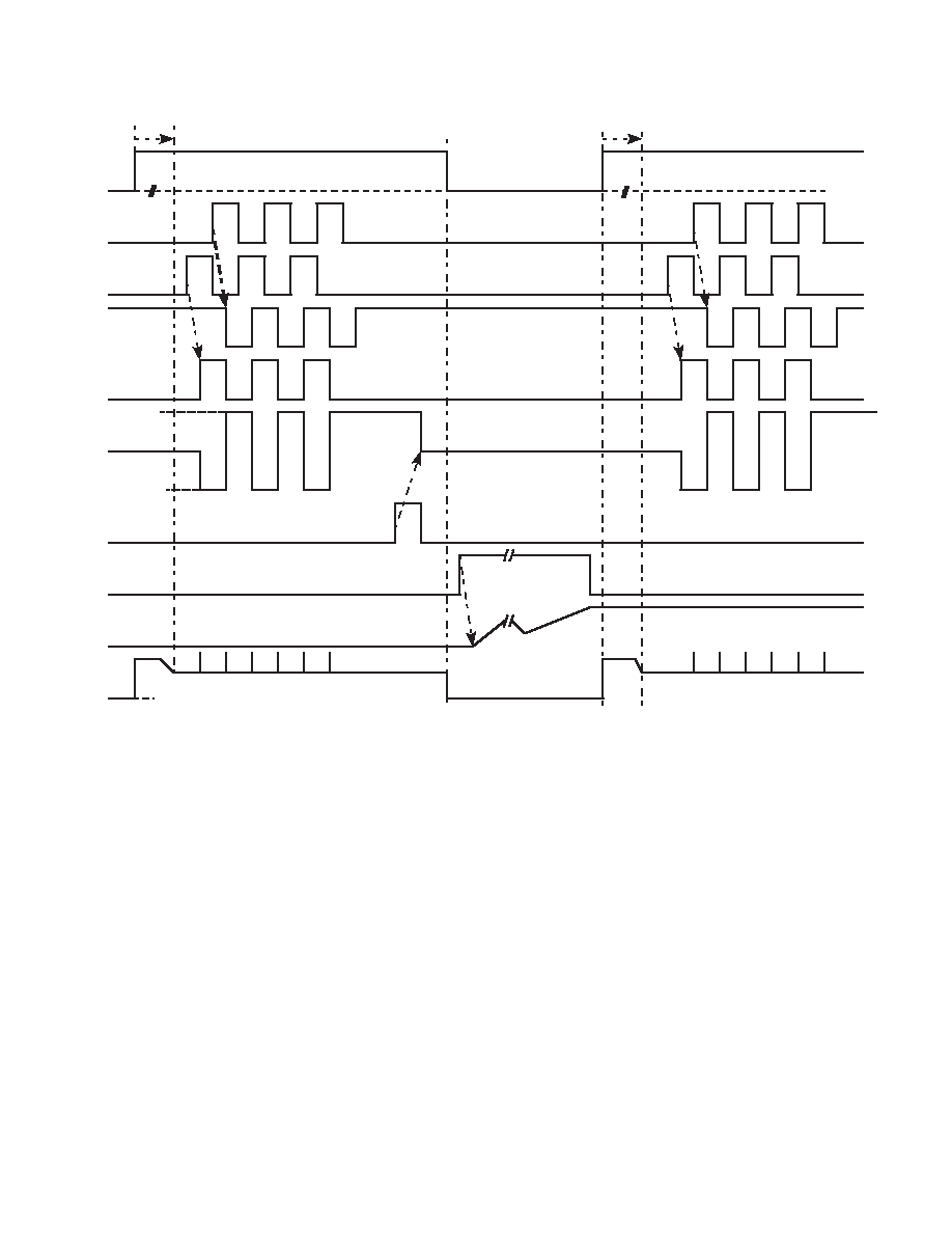
HV732 Timing Diagram
EN
P
IN
N
IN
N
DR
P
DR
HV
out
DAMP
1us
1us
CLAMP
V
PP
30Us
V
PP
V
NN
0V
I
AVDD
0.175mA
2mA
1.5mA
30Us
8
NR040506
HV732
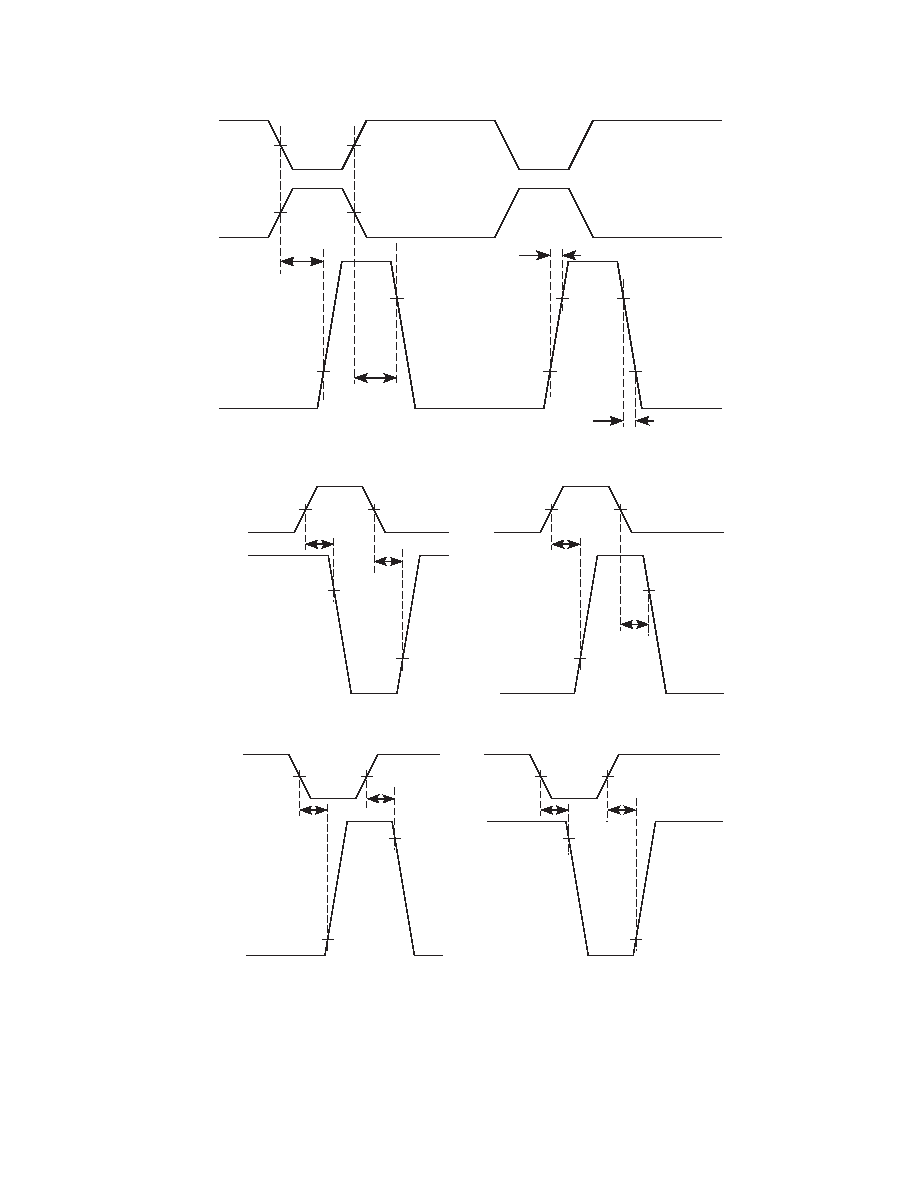
HV732 DAMP Switching Time Diagram
HV732 Clamp Switching Time Diagram
t
DMPON(N)
50%
10%
50%
90%
DAMP
DAMP
OUT
0V
t
DMPOFF(N)
V
NN
t
DMPON(P)
50%
10%
50%
90%
t
DMPOFF(P)
0V
V
PP
t
CLPON(P)
50%
10%
50%
90%
CLAMP
HV
OUT
0V
t
CLPOFF(P)
V
NN
t
CLPON(N)
50%
10%
50%
90%
t
CLPOFF(N)
0V
V
PP
HV732 TX Switching Time Diagram
t
dr
50%
10%
50%
90%
P
IN
N
IN
t
df
HV
OUT
V
NN
V
PP
t
r
10%
90%
t
f
90%
10%
9
NR040506
HV732
Pin Description
Pin
Function
Description
1
DMPO
Output of low voltage drive buffer for P-channel damp, 10nF external cap to pin 34 (DMPI)
2
GND
Drive power ground
3
N
DR
Output of low voltage drive buffer for N-DMOS, 10nF external cap to pin 9 (NGATE)
4
V
DD
Positive voltage supply for drive circuitry (+12V)
5
VDD
Positive voltage supply for drive circuitry (+12V)
6
V
SUB
Substrate connection of control / driver die chip (connected to the most positive supply, V
PP
)
7
RGND
N
Ground return of damp N-DMOS source
8
OUT
N
Output of damp N-DMOS drain (open drain output)
9
NGATE
Gate input of the high voltage N-DMOS, 10nF external cap from pin 3 (N
DR
)
10
V
NN
Negative high voltage power supply (-100V)
11
V
NN
Negative high voltage power supply (-100V)
12
V
NN
Negative high voltage power supply (-100V)
13
V
NN
Negative high voltage power supply (-100V)
14
V
NN
Negative high voltage power supply (-100V)
15
TX
N
Output of the high voltage N-DMOS drain (open drain output)
16
TX
N
Output of the high voltage N-DMOS drain (open drain output)
17
NC
No connection
18
TX
P
Output of the high voltage P-DMOS drain (open drain output)
19
TX
P
Output of the high voltage P-DMOS drain (open drain output)
20
V
PP
Positive high voltage power supply (+100V)
21
V
PP
Positive high voltage power supply (+100V)
22
V
PP
Positive high voltage power supply (+100V)
23
V
PP
Positive high voltage power supply (+100V)
24
V
PP
Positive high voltage power supply (+100V)
25
PGATE
Gate input of the high voltage P-DMOS, 10nF external cap from pin 31 (P
DR
)
26
OUT
P
Damp P-DMOS drain (open drain output)
27
RGND
P
Ground return of damp P-DMOS
28
V
SUB
Substrate connection of control / driver die chip (connected to the most positive supply, V
P
P)
29
V
DD
Positive voltage supply for drive circuitry (+12V)
30
V
DD
Positive voltage supply for drive circuitry (+12V)
31
P
DR
Output of low voltage drive buffer for P-DMOS, 10nF external cap to pin 25 (PGATE)
32
GND
Drive power ground
33
GND
Drive power ground
34
DMPI
Connects to damp power P-DMOS gate, 10nF cap to pin 1 (DMPO)
35
P
IN
Input logic control of the high voltage P-DMOS pin 18 &19 (TX
P)
, Hi = on, Low = off
36
V
LN
Negative low voltage power supply (≠5V)
37
AV
DD
Positive analog voltage power supply (+12V)
38
AGND
Analog signal ground (0V)
39
V
SUB
Substrate connection of control / driver chip (connected to the most positive supply)
40
EN
Control / drive chip power enable Hi = on, Low = off
41
DAMP
Input of damp control on both pin 26 (OUT
P
) and pin 8 (OUT
N
), Hi = on, Low = off
42
CLAMP
Input of clamp switches on both gates of output P-DMOS and N-DMOS, Hi = on, Low = off
43
V
LL
Positive voltage supply of low voltage logic (+1.8V to +5V)
44
N
IN
Input logic control of the high voltage N-DMOS pin 15 & 16 (TX
N
), Hi = on, Low = off
Note: The three thermal slabs on the bottom of the package must be externally connected PAD1 to V
SUB
, PAD2 to TX
N
, and PAD3 to TX
P
.
Supertex inc.
1235 Bordeaux Drive, Sunnyvale, CA 94089
TEL: (408) 222-8888 / FAX: (408) 222-4895
www.supertex.com
©2006 Supertex inc. All rights reserved. Unauthorized use or reproduction is prohibited.
Supertex inc.
does not recommend the use of its products in life support applications, and will not knowingly sell its products for use in such applications, unless it receives an adequate
"product liability indemnification insurance agreement". Supertex does not assume responsibility for use of devices described and limits its liability to the replacement of the devices
determined defective due to workmanship. No responsibility is assumed for possible omissions or inaccuracies. Circuitry and specifications are subject to change without notice. For the latest
product specifications, refer to the Supertex website: http//www.supertex.com.
10
Doc.# DSFP - HV732
NR040506
HV732
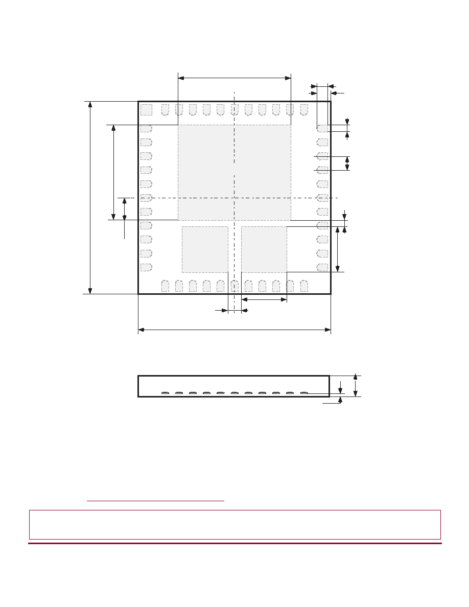
44-Lead QFN (K6) Package Outline
(The package drawing(s) in this data sheet may not refl ect the most current specifi cations. For the latest package outline
information go to
http://www.supertex.com/packaging.html
.)
1
44
1.77 [.070]
1.57 [.062]TYP
0.36 [.014]
0.26 [.010]
1.77 [.070]
1.57 [.062]TYP
0.53 [.021]
0.48 [.019]
0.28 [.011]
0.23 [.009]
0.45 [.018]
0.35 [.014]
0.38 [.015]
0.28 [.011]
0.51 [.020]
0.41 [.016]
3.35 [.141]
3.37 [.133]
4.40 [.173]
4.20 [.165]
0.74 [.029]
0.69 [.027]
7.13 [.281]
6.87 [.271]
7.13 [.281]
6.87 [.271]
PAD2
PAD3
11
12
22
Note:
1. Dimensions in mm. [Inch]
2. Radius is 0.127mm
3. Three thermal slabs on the bottom of the package
must be externally connected PAD1 to V
SUB
,
PAD2 to TX
N
, and PAD3 to TX
P
.
0.05 [.002]
0.00 [.000]
1.00 [.039]
0.85 [.033]
(N)
(P)
Top View
PAD1