1
HV826
High Voltage EL Lamp Driver
Features
1.8V to 3.5V operating supply voltage
DC to AC conversion
Adjustable output frequency
Adjustable switch frequency
Output voltage regulation
Enable/disable function
General Description
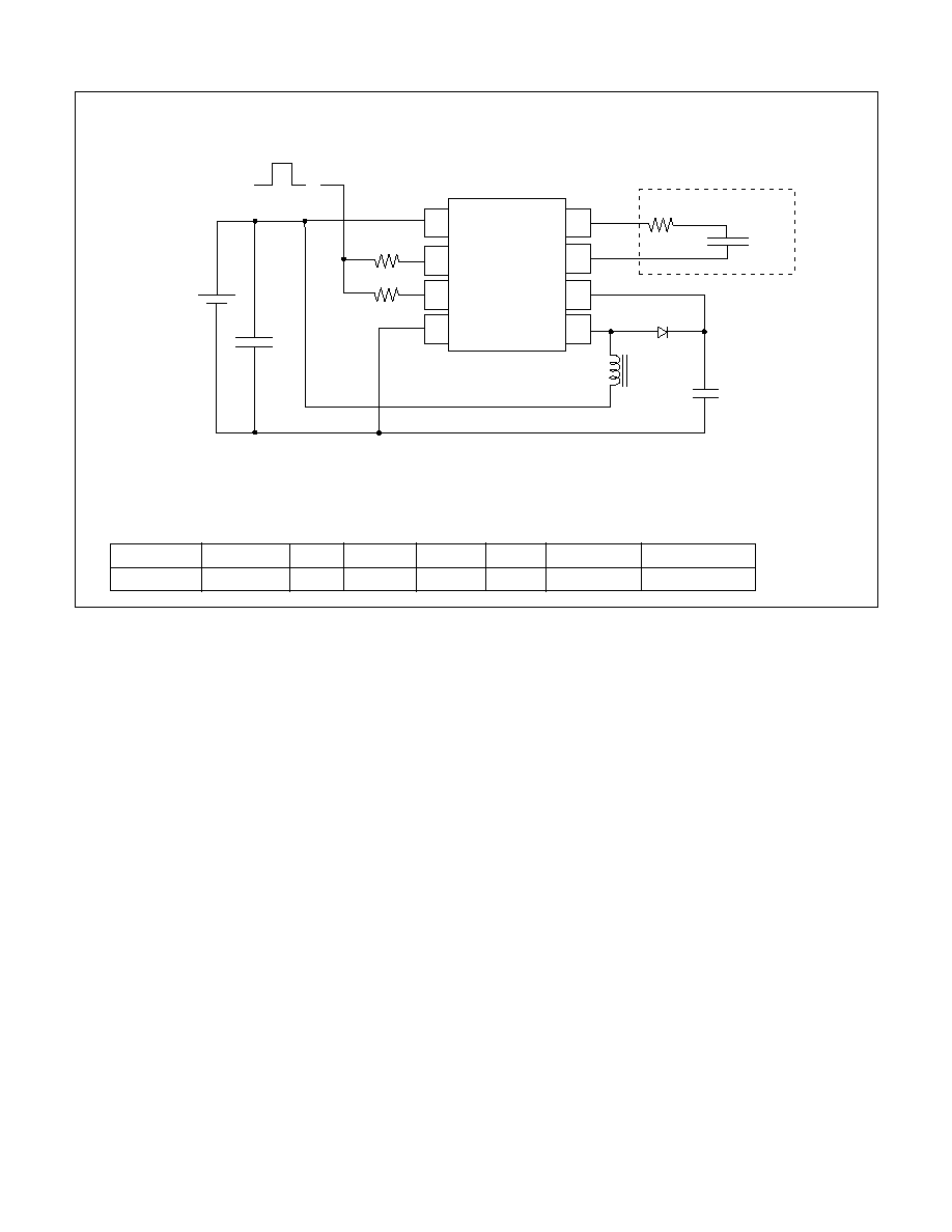
The Supertex HV826 is a high voltage driver designed for driving
EL lamps. The input supply voltage range is from 1.8V to 3.5V.
The device uses a single inductor and a minimum number of
passive components. The nominal regulated output voltage that
is applied to the EL lamp is
±80V. The chip can be enabled/
disabled by connecting the resistor on R
SW-OSC
to V
DD
/ground.
The HV826 has two internal oscillators, a switching MOSFET,
and a high voltage EL lamp driver. The frequency for the
switching MOSFET is set by an external resistor connected
between the R
SW-osc
pin and the supply pin V
DD
. The EL lamp
driver frequency is set by an external resistor connected be-
tween R
EL-osc
pin and the V
DD
pin. An external inductor is
connected between the L
X
and V
DD
pins. A 0.01-0.1
µF capacitor
is connected between C
S
and ground. The EL lamp is connected
between V
A
and V
B
.
The switching MOSFET charges the external inductor and
discharges it into the capacitor at C
S
. The voltage at C
S
will start
to increase. Once the voltage at C
S
reaches a nominal value of
80V, the switching MOSFET is turned OFF to conserve power.
The outputs V
A
and V
B
are configured as an H bridge and are
switching in opposite states to achieve 160V peak-to-peak
across the EL lamp.
Applications
Mobile cellular phones
Pagers
Portable Transceivers
Remote Control Units
Calculators
Absolute Maximum Ratings*
Supply Voltage, V
DD
-0.5V to +4.5V
Output Voltage, V
Cs
-0.5V to +100V
Operating Temperature Range
-25
∞ to +85∞C
Storage Temperature Range
-65
∞C to +150∞C
MSOP-8 Power Dissipation
250mW
SO-8 Power Dissipation
400mW
Note:
*All voltages are referenced to GND.
Package Options
Device
MSOP-8
SO-8
Die
HV826
HV826MG*
HV826LG
HV826X
* Product supplied on 2500 piece carrier tape reels.
Ordering Information
Pin Configuration
V
DD
V
A
R
SW-osc
V
B
R
EL-osc
C
S
Gnd
L
X
1
2
3
4
8
7
6
5
MSOP-8
and
SO-8
Top View
11/12/01
Supertex Inc. does not recommend the use of its products in life support applications and will not knowingly sell its products for use in such applications unless it receives an adequate "products liability
indemnification insurance agreement." Supertex does not assume responsibility for use of devices described and limits its liability to the replacement of devices determined to be defective due to
workmanship. No responsibility is assumed for possible omissions or inaccuracies. Circuitry and specifications are subject to change without notice. For the latest product specifications, refer to the
Supertex website: http://www.supertex.com. For complete liability information on all Supertex products, refer to the most current databook or to the Legal/Disclaimer page on the Supertex website.
2
HV826
Symbol
Parameter
Min
Typ
Max
Units
Conditions
R
DS(on)
On-resistance of switching transistor
7.0
I=100mA
V
Cs
Max. output regulation voltage
75
80
85
V
V
DD
=1.8V to 3.5V
V
A-B
Max. of differential output voltage
150
160
170
V
V
DD
=1.8V to 3.5V
across lamp
I
DDQ
Quiescent V
DD
supply current
100
nA
R
SW-osc
= Low
I
DD
Input current going into the V
DD
pin
150
µA
V
DD
=1.8V to 3.5V. See Figure 1.
I
IN
Input current including inductor current
35
45
mA
V
IN
=1.5V. See Figure 1.
V
CS
Output voltage on V
CS
65
70
V
V
IN
=1.5V. See Figure 1.
f
EL
V
A-B
output drive frequency
300
375
450
Hz
V
IN
=1.5V. See Figure 1.
f
SW
Switching transistor frequency
80
KHz
V
IN
=1.5V. See Figure 1.
D
Switching transistor duty cycle
88
%
See figure 1.
Electrical Characteristics
DC Characteristics
(Over recommended operating conditions unless otherwise specified, T
A
=25
∞C)
Symbol
Parameter
Min
Typ
Max
Units
Conditions
V
DD
Supply voltage
1.8
3.5
V
f
EL
V
A-B
output drive frequency
60
1000
KHz
T
A
Operating temperature
-25
85
∞C
Recommended Operating Conditions
Symbol
Parameter
Min
Typ
Max
Units
Conditions
EN-L
Logic input low voltage
0
0.5
V
V
DD
=1.8V to 3.5V
EN-H
Logic input high voltage
V
DD
-0.5
V
DD
V
V
DD
=1.8V to 3.5V
Enable/Disable Function Table