1
HV831/HV839
High Voltage Dual EL Lamp Driver
HV831/HV839
03/24/03
Supertex Inc. does not recommend the use of its products in life support applications and will not knowingly sell its products for use in such applications unless it receives an adequate "products liability
indemnification insurance agreement." Supertex does not assume responsibility for use of devices described and limits its liability to the replacement of devices determined to be defective due to
workmanship. No responsibility is assumed for possible omissions or inaccuracies. Circuitry and specifications are subject to change without notice. For the latest product specifications, refer to the
Supertex website: http://www.supertex.com. For complete liability information on all Supertex products, refer to the most current databook or to the Legal/Disclaimer page on the Supertex website.
General Description
The Supertex HV831 and HV839 are high voltage drivers
designed for driving two EL lamps with a combined area of 3.5
square inches. The input supply voltage range is from 2.0V to
5.0V. The device is designed to reduce the amount of audible
noise emitted by the lamp. These devices use a single inductor
and a minimum number of passive components. The nominal
regulated output voltage that is applied to the EL lamp is
±
80V for
HV831 and
±
90V for HV839. HV839 will provide higher brightness
due to its higher output voltage regulation. The chip can be
disabled by connecting C
1
and C
2
(pins 1 and 4) to GND.
The HV831 and HV839 have an internal oscillator, a switching
MOSFET, and two high voltage EL lamp drivers. The frequency
for the switching MOSFET is set by an external resistor connected
between the R
SW-OSC
pin and the voltage supply pin V
DD
. The EL
lamp driver frequency is set by dividing the MOSFET switching
frequency by 128. An external inductor is connected between
the L
X
and V
DD
pins. Depending on EL lamp size, 0.001 to
0.01
µ
F, 100V capacitor is connected between C
S
and Ground.
The EL lamps are connected between EL
1
to Com and EL
2
to
Com.
Two input control pins (C
1
and C
2
) are available to select various
modes of the device. The device can be disabled by applying
GND to both C
1
and C
2
(pins 1 and 4). C
1
and C
2
control the ON/
OFF states of EL
1
and EL
2
, respectively. EL
1
will be ON when C
1
is at V
DD
and EL
2
will be ON when C
2
is at V
DD
. EL
1
and EL
2
will
be ON when both C
1
and C
2
are at V
DD
.
The switching MOSFET charges the external inductor and
discharges it into the capacitor at C
S
. The voltage at C
S
will start
to increase. Once the voltage at C
S
reaches a nominal value of
80V for HV831 and 90V for HV839, the switching MOSFET is
turned off to conserve power. The outputs EL
1
to Com and EL
2
to Com are configured as H bridges and are switching in opposite
states to achieve 160/180V across the EL lamp for HV831/
HV839.
Features
Independent input control for lamp selection
Split supply capability
Patented output timing
One minature inductor to power both lamps
150nA shutdown current
Wide input voltage range (2.0V to 5.0V)
Output voltage regulation
No SCR output
Small package 10-pin MSOP dual EL driver IC
Low audible noise via Patent Pending technology
Applications
Mobile cellular phones, dual display
Keypad and LCD backlighting
Portable instrumentation
Dual segment lamps
Hand held wireless communication devices
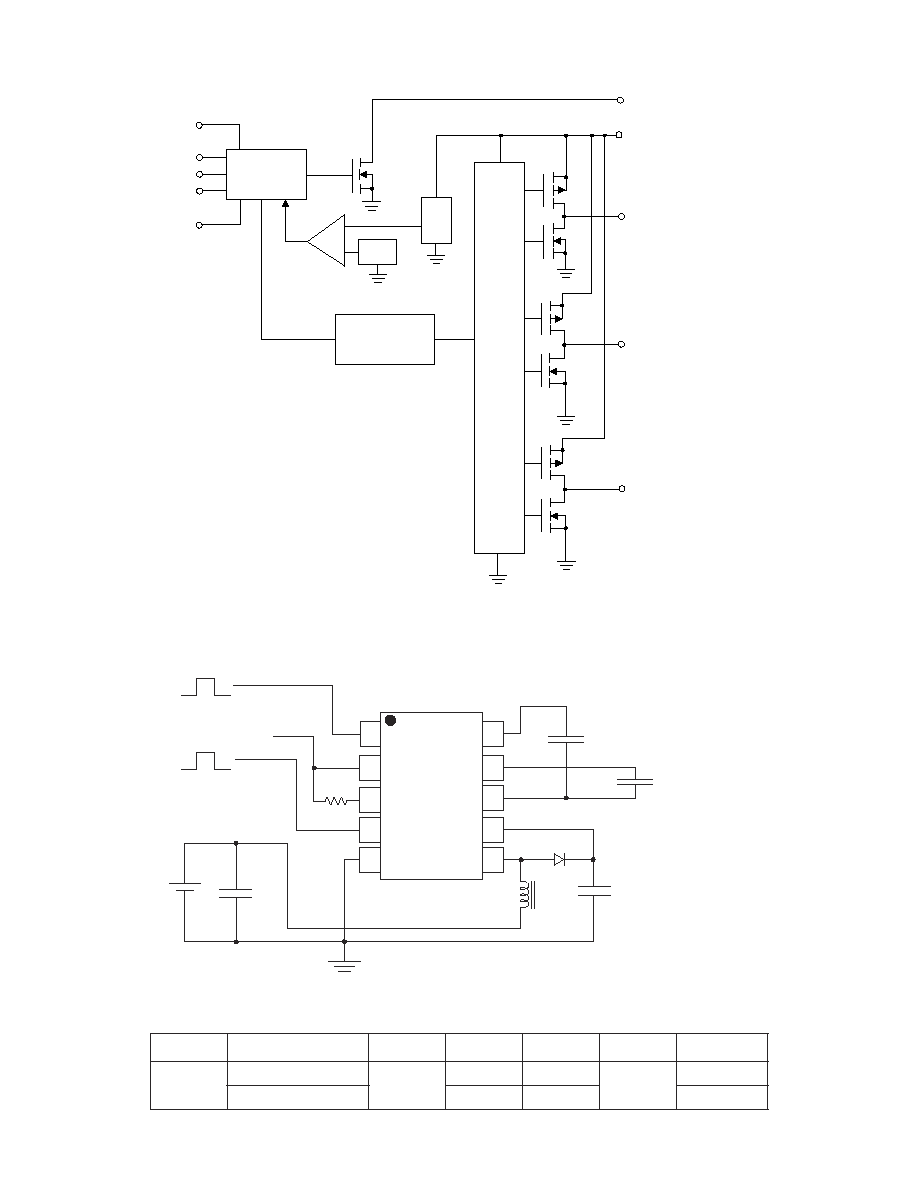
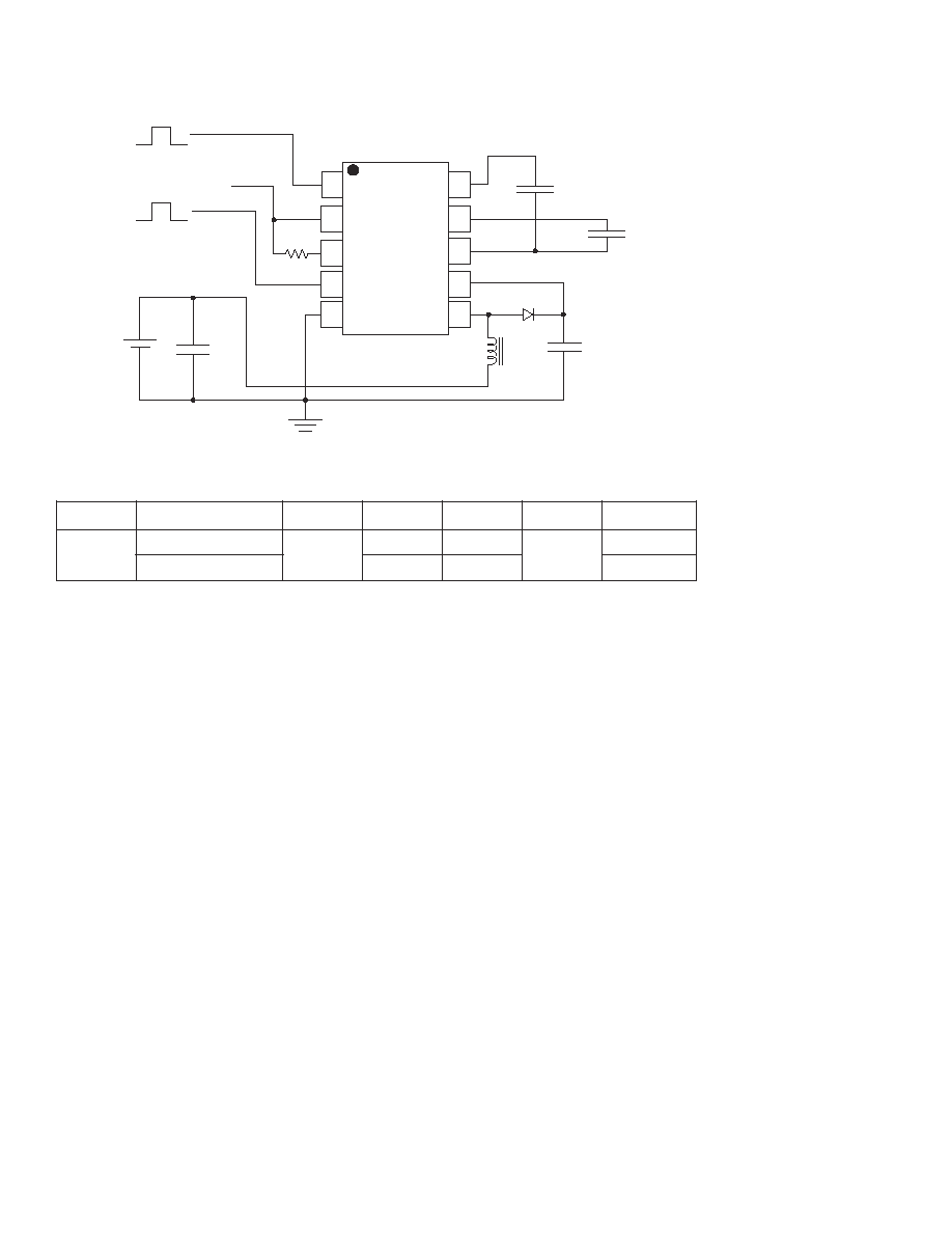
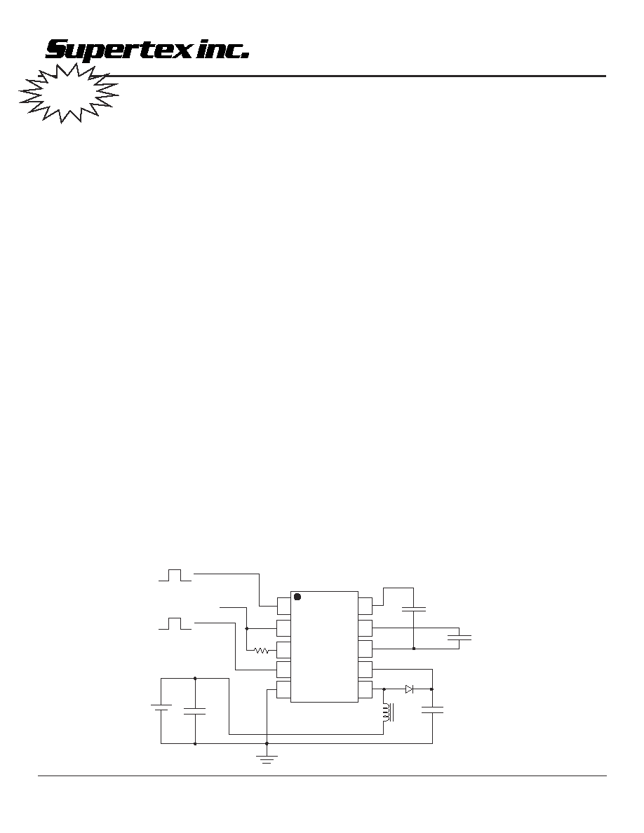
Typical Application Circuit
EL Lamp 1
+
_
9
7
6
HV831MG/
HV839MG
8
V
IN
EL Lamp 2
L
X
EL
1
V
DD
C
2
GND
L
X
C
S
Com
EL
2
1
2
3
4
10
5
C
1
R
SW-OSC
V
DD
0
V
DD
0
V
DD
Cs
100V
1N914
Demo Kit
Available
2
HV831/HV839
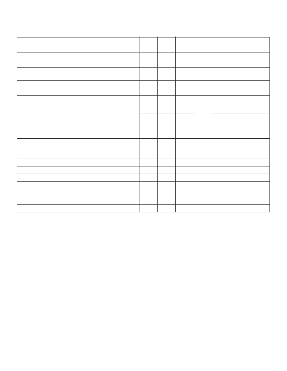
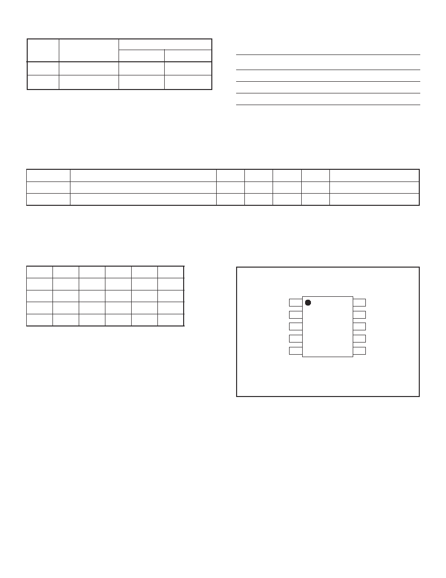
Function Table
C
1
C
2
L
E
1
L
E
2
m
o
C
C
I
0
0
Z
I
H
Z
I
H
Z
I
H
F
F
O
0
1
Z
I
H
N
O
N
O
N
O
1
0
N
O
Z
I
H
N
O
N
O
1
1
N
O
N
O
N
O
N
O
Absolute Maximum Ratings**
Supply voltage, V
DD
-0.5V to 7.5V
Output voltage, V
CS
-0.5V to +120V
Operating Temperature Range
-40
∞
C to +85
∞
C
Storage Temperature Range
-65
∞
C to +150
∞
C
10 Pin MSOP Power Dissipation
250mW
** All voltages are referenced to ground.
Pin Configuration
top view
MSOP-10
1
2
3
4
5
10
9
8
7
6
C
1
V
DD
R
SW-OSC
C
2
GND
EL
1
EL
2
Com
V
CS
L
X
l
o
b
m
y
S
r
e
t
e
m
a
r
a
P
n
i
M
p
y
T
x
a
M
s
t
i
n
U
s
n
o
i
t
i
d
n
o
C
V
D
D
e
g
a
t
l
o
v
y
l
p
p
u
S
0
.
2
0
.
5
V
T
A
e
r
u
t
a
r
e
p
m
e
t
g
n
i
t
a
r
e
p
O
0
4
-
5
8
C
∞
Recommended Operating Conditions
Ordering Information
Device
Output Regulation
Voltage
MSOP-10
Die
HV831
80V
HV831MG*
HV831X
HV839
90V
HV839MG*
HV839X
* Product supplied on 2500 piece carrier tape reels only.
Package Options
8
HV831/HV839
1235 Bordeaux Drive, Sunnyvale, CA 94089
TEL: (408) 222-8888 ∑ FAX: (408) 222-4895
www.supertex.com
03/24/03rev.6
©2003 Supertex Inc. All rights reserved. Unauthorized use or reproduction prohibited.
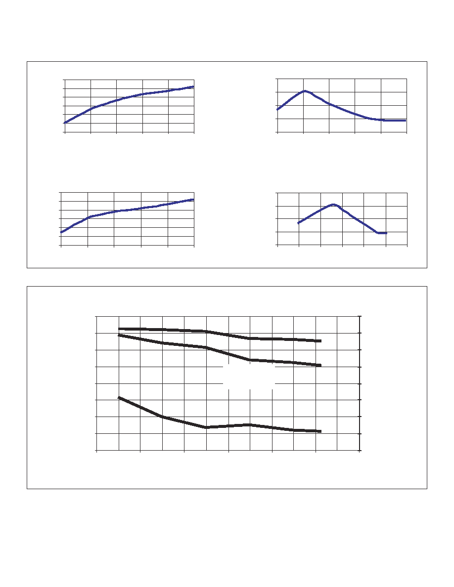
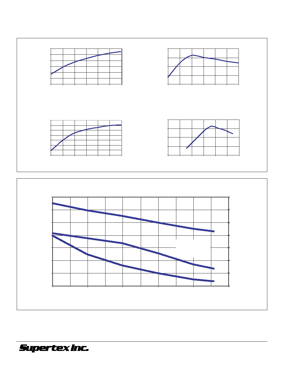
Typical HV839 Performance Curves for Figure 2
(When driving both EL Lamps)
(EL1 Lamp = 1.3 in
2
, EL2 Lamp = 0.93 in
2
, V
DD
= 3.0V).
Iin vs Vin
Vcs vs Vin
Brightness vs Vin
Iin vs Vcs
Brightness (ft-lm)
Iin (mA)
Iin (mA)
60
65
70
75
80
85
90
2.0
2.5
3.0
3.5
4.0
4.5
5.0
Vin (V)
30
35
40
45
50
2.0
2.5
3.0
3.5
4.0
4.5
5.0
Vin (V)
30
35
40
45
50
60
65
70
75
80
85
90
Vcs (V)
2
4
6
8
10
12
14
16
2.0
2.5
3.0
3.5
4.0
4.5
5.0
Vin (V)
Vcs (V)
Iin, Vcs, Brightness vs Inductor Value
Inductor Value (
µ
H)
lin (mA), Vcs (V)
Brightness (ft-lm)
20
30
40
50
60
70
80
90
100
200
300
400
500
600
4
6
8
10
12
14
16
18
Vcs
Brightness
(measured on
EL1 lamp)
lin