 | –≠–ª–µ–∫—Ç—Ä–æ–Ω–Ω—ã–π –∫–æ–º–ø–æ–Ω–µ–Ω—Ç: HV841MG-G | –°–∫–∞—á–∞—Ç—å:  PDF PDF  ZIP ZIP |

Supertex inc.
HV841
High Voltage Dual EL Lamp Driver
Supertex inc.
∑
1235 Bordeaux Drive, Sunnyvale, CA 94089
∑
Tel: (408) 222-8888
∑
FAX: (408) 222-4895
∑
www.supertex.com
1
NR033106
Initial Release
Features
Independent input control for lamp selection
Split supply capability
Patented output timing
One miniature inductor to power both lamps
Low shutdown current
Wide input voltage range 2.0V to 5.8V
Output voltage regulation
No SCR output
Available in small packages (10-lead MSOP and
10-lead DFN/MLP)
Applications
Mobile cellular phones, dual display
Keypad and LCD backlighting
Portable instrumentation
Dual segment lamps
Hand held wireless communication devices
General Description
The Supertex HV841 is a high voltage driver designed for driving
two EL lamps with a combined area of 3.5 square inches. The input
supply voltage range is from 2.0V to 5.8V. The device is designed to
reduce the amount of audible noise emitted by the lamp. This device
uses a single inductor and minimum number of passive components
to drive two EL lamps. The nominal regulated output voltage of
±100V is applied to the EL lamps. The chip can be enabled/ disabled
by connecting C
1
and C
2
(pins 1 and 4) to V
EN
/ Ground.
The HV841 has an internal oscillator, a switching MOSFET, and two
high voltage EL lamp drivers. An external resistor connected between
the R
SW-OSC
and the voltage supply pin V
DD
sets the frequency for the
switching MOSFET. The EL lamp driver frequency is set by dividing
the MOSFET switching frequency by 128. An external inductor is
connected between the L
X
and the V
DD
pins. Depending on the EL
lamp size, a 1.0 to 10.0nF, 200V capacitor is connected between C
S
and Ground. The two EL lamps are connected between EL
1
to Com
and EL
2
to Com.
The switching MOSFET charges the external inductor and discharges
it into the capacitor at C
S
. The voltage at C
S
increases. Once the
voltage at C
S
reaches a nominal value of 100V, the switching
MOSFET is turned off to conserve power. The outputs EL
1
to Com
and EL
2
to Com are confi gured as H bridges and switch in opposite
states to achieve 200V across the EL lamp.
Typical Application Circuit
D
C
S
+
-
+
-
1
2
3
4
5
6
7
8
9
10
L
X
V
EN
= ON
0 = OFF
V
EN
= ON
0 = OFF
V
DD
C
DD
V
IN
C
IN
R
SW-OSC
HV841MG-G/
HV841K6-G
EL Lamp 2
1
EL Lamp 1
1
V
DD
Com
C2
GND
EL
2
L
X
C
S
EL
1
C
1
R
SW-OSC
~
1 The bigger sized lamp should be tied to EL1 and the smaller
sized lamp to EL2 terminals (pins 10 and 9 respectively)
2
NR033106
HV841
Recommended Operating Conditions
Symbol
Parameter
Min
Typ
Max
Units
Conditions
V
DD
Supply Voltage
2.0
5.8
V
T
A
Operating Temperature
-40
85
o
C
Ordering Information
DEVICE
Package Options
DFN/MLP-10
1
MSOP-10
2
HV841
HV841K6-G
HV841MG-G
Absolute Maximum Ratings*
Supply Voltage, V
DD
-0.5 to +7.5V
Supply Voltage, V
CS
-0.5 to +120V
Operating Ambient Temperature Range
-40∞C to +85∞C
Storage Temperature Range
-65∞ to +150∞C
*Absolute Maximum Ratings are those values beyond which damage to the
device may occur. Functional operation under these conditions is not implied.
Continuous operation of the device at the absolute rating level may affect
device reliability. All voltages are referenced to device ground, Gnd
1 Product supplied on 3000 piece carrier tape reels only
2 Product supplied on 2500 piece carrier tape reels only
-G indicates package is RoHS compliant (`Green')
C
1
C
2
EL
1
EL
2
Com
IC
0
0
Hi Z
Hi Z
Hi Z
OFF
0
1
Hi Z
ON
ON
ON
1
0
ON
Hi Z
ON
ON
1
1
ON
ON
ON
ON
Function Table
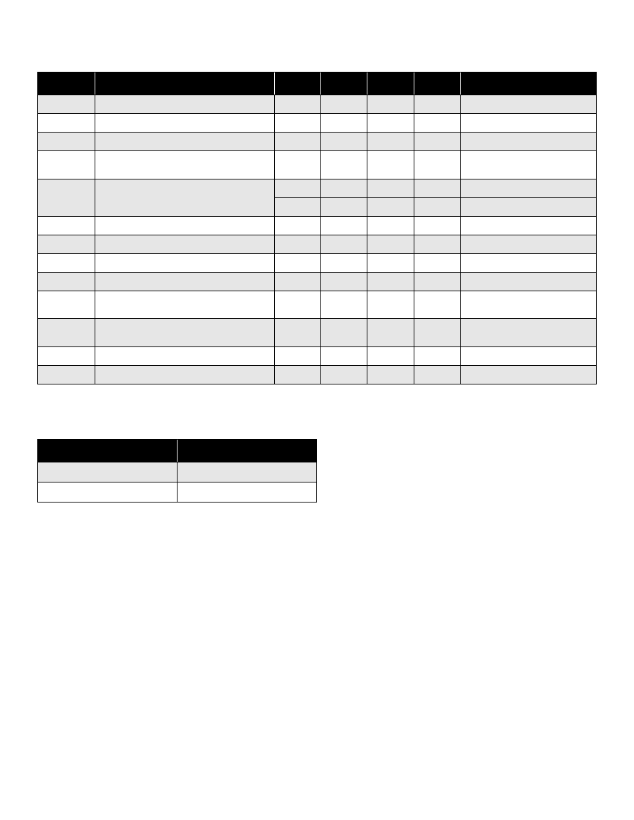
Pin Confi guration
Pin1
HV841K6-G
C
1
C
2
C
S
L
X
V
DD
COM
EL
1
EL
2
GND
R
SW-OSC
HV841MG-G
V
DD
Com
C
2
GND
EL
2
L
X
C
S
EL
1
1
2
3
4
5
6
7
8
9
10
C
1
R
SW-OSC
Top View: MSOP-10
Top View: DFN/MLP-10
(Pads are on the bottom of the package.)
Note: Packages are not drawn to scale.
3
NR033106
HV841
Symbol
Parameter
Min
Typ
Max
Units
Conditions
R
DS(ON)
On-resistance of switching transistor
-
-
6.0
I = 100mA
V
DD
Input Voltage Range
2.0
-
5.8
V
---
V
CS
Output regulation voltage
90
100
110
V
V
DD
= 2.0V to 5.8V
V
DIFF
Differential output peak to peak voltage
(EL
1
to Com, EL
2
to Com)
180
200
220
V
V
DD
= 2.0V to 5.8V
I
DDQ
Quiescent V
DD
supply current
-
-
150
nA
C
1
= C
2
= 0 to 0.1V
-
-
500
nA
C
1
= C
2
= 0.1 to 0.3V
I
DD
Input current into the V
DD
pin
-
190
µA
V
DD
= 2.0V to 5.8V
f
EL
V
DIFF
output drive frequency
215
244
273
Hz
V
IN
= 3.0V. See Figure 1.
f
SW
Switching transistor frequency
27.5
31.2
34.9
kHz
V
IN
= 3.0V. See Figure 1.
D
Switching Transistor Duty cycle
85
-
89
%
---
I
IL
Input logic low current going into the
control pin
-
-
-0.6
µA
V
DD
= 2.0V to 5.8V
I
IH
Input logic low current going into the
control pin
-
-
0.6
µA
V
DD
= 2.0V to 5.8V
V
EN-L
Logic input low voltage
0
-
0.3
V
---
V
EN-H
Logic input high voltage
1.5
-
V
DD
V
---
Package
JA
MSOP-10
400
o
C/W
DFN/MLP-10
60
o
C/W
Thermal Resistance
(Mounted on FR4 board, 25mm x 25mm x 1.57mm)
Electrical Characteristics
DC Characteristics
(Over operating conditions unless otherwise specifi ed, T
A
= 25∞C)
4
NR033106
HV841
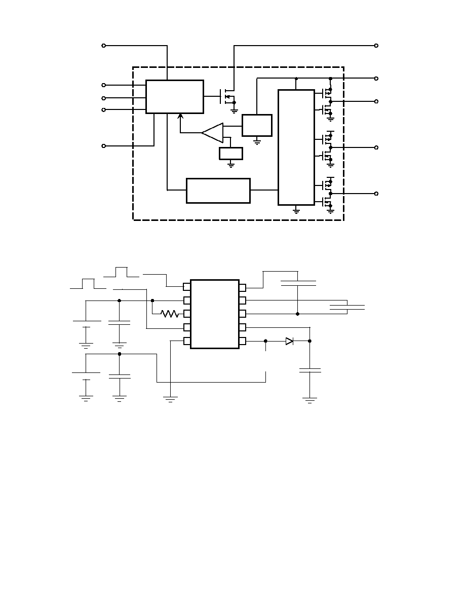
Functional Block Diagram
Figure 1: Test Circuit
Vcs
Vcs
Disable
EL
1
EL
2
COM
R
SW-OSC
C
S
Lx
V
DD
C
1
C
2
GND
Output
Drivers
Logic Control &
Divide by 128
Control Logic
& Switch-Osc
-
+
V
SENSE
V
REF
BAS21
1
+
-
+
-
1
2
3
4
5
6
7
8
9
10
330
µH
2
V
EN
= ON
0 = OFF
V
EN
= ON
0 = OFF
V
DD
V
IN
470 k
HV841MG-G/
HV841K6-G
EL Lamp 2 (1.6 in
2
)
3
V
DD
Com
C
2
GND
EL
2
L
X
C
S
EL
1
C
1
R
SW-OSC
0.1
µF
4.7
µF
3.3 nF, 200V
EL Lamp 1 (1.9 in
2
)
3
1 or any (equivalent or better)
> 120V, fast recovery diode
2 Murata LQH4CN331K04
3 The bigger sized lamp should be tied to EL1 and the smaller
sized lamp to EL2 terminals (pins 10 and 9 respectively)
~
5
NR033106
HV841
Pin Confi guration and Description
Pin #
Name
Function
1
C
1
Enable input signal for EL lamp 1. Logic high will turn ON the EL lamp 1 and logic low will turn it OFF. Refer to the
Function Table.
2
V
DD
Input supply voltage pin.
3
R
SW-OSC
External resistor connection to set both the switching MOSFET frequency and EL Lamp frequency. The external
resistor should be connected between this pin and the V
DD
pin. The EL lamp frequency is switching frequency
divided by 128.
The switching frequency increases as the value of R
SW-OSC
decreases. A 470k
resistor will provide a switching
frequency of 31.2 kHz, and an EL lamp frequency of 244 Hz. To change the frequency to f
SW1
, the value of the
resistor R
SW-OSC1
can be determined as R
SW-OSC1
= (470k x 31.2k) / f
SW1
.
4
C
2
Enable input signal for EL lamp 2. Logic high will turn ON the EL lamp 2 and logic low will turn it OFF. Refer to the
Function Table.
5
GND
IC Ground Pin.
6
L
X
External inductor connection to boost the low input voltage using inductive fl yback. Connect an inductor
between V
IN
and this pin. Also connect a high voltage fast recovery diode between this pin and the C
S
pin. The anode of the diode needs to be connected to the L
X
pin and the cathode to the C
S
pin. In general,
small valued inductors, which can handle more current, are more suitable for driving large sized lamps.
As the inductor value decreases, the switching frequency should be increased to avoid saturation.
When the switching MOSFET is turned ON, the inductor is being charged. When the MOSFET is turned OFF, the
energy stored in the inductor is transferred to the high voltage capacitor connected at the C
S
pin.
7
C
S
Connect a 200V capacitor between this pin and GND. This capacitor stores the energy transferred from the
inductor.
8
Com
Common connection for both EL lamps. Connect one end of both the lamps to this pin.
9
EL
2
EL lamp 2 connection. For optimum performance, the smaller of the two lamps should be connected to this pin.
10
EL
1
EL lamp 1 connection. For optimum performance, the larger of the two lamps should be connected to this pin.
6
NR033106
HV841
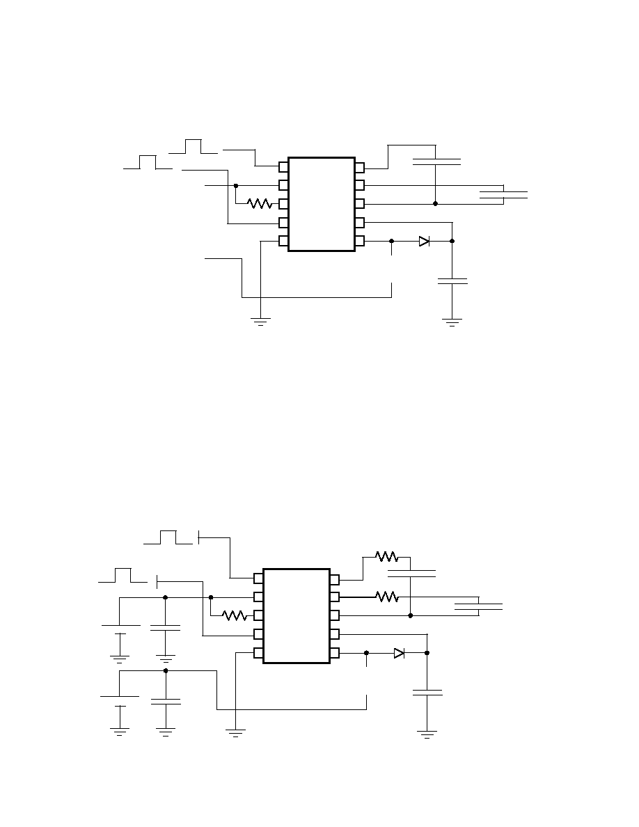
The HV841 can be used in applications operating from a battery
where a regulated voltage is available. This is shown in Figure
2. The regulated voltage can be used to drive the internal logic
of HV841. The amount of current used to drive the internal logic
is less than 190µA. Therefore, the regulated voltage could easily
provide the current without being loaded down.
Figure 2: Split Supply Confi guration
D
C
S
1
2
3
4
5
6
7
8
9
10
L
X
V
EN
= ON
0 = OFF
V
EN
= ON
0 = OFF
Regulated Voltage = V
DD
R
SW-OSC
HV841MG-G/
HV841K6-G
EL Lamp 2
1
EL Lamp 1
1
V
DD
Com
C
2
GND
EL
2
L
X
C
S
EL
1
C
1
R
SW-OSC
Battery Voltage = V
IN
~
1 The bigger sized lamp should be tied to EL1 and the smaller
sized lamp to EL2 terminals (pins 10 and 9 respectively)
This section describes a method (patented) developed at Supertex
to reduce the audible noise emitted by the EL lamps used in
application sensitive to audible noise. The waveform takes the
shape of approximately 2RC time constants for rising and 2RC time
constants for falling, where C is the capacitance of the EL lamp,
and R is the external resistor, R
SER
connected in series with the EL
lamp.
Figure 3 shows a general circuit schematic that uses the series
resistors, R
SER1
and R
SER2
, for each of the EL lamps. R
SER1
and
R
SER2
are connected in series with the EL lamp. The audible noise
can be set a desirable level by selecting the resistances for R
SER1
and R
SER2
. It is important to note that addition of these external
resistors will reduce the voltage across the EL lamp, and hence the
brightness of the EL lamp.
Figure 3: Typical Application Circuit For Audible Noise Reduction
Audible Noise Reduction
D
C
S
+
-
+
-
1
2
3
4
5
6
7
8
9
10
L
X
ON = V
EN
OFF = 0
V
DD
C
DD
V
IN
C
IN
R
SW-OSC
HV841MG-G/
HV841K6-G
EL Lamp 2
1
EL Lamp 1
1
V
DD
Com
C
2
GND
EL
2
L
X
C
S
EL
1
C
1
R
SW-OSC
R
SER2
R
SER1
ON = V
EN
OFF = 0
Enable 1
Enable 2
~
1 The bigger sized lamp should be tied to EL1 and the smaller
sized lamp to EL2 terminals (pins 10 and 9 respectively)
Split Supply Confi guration
Supertex inc.
1235 Bordeaux Drive, Sunnyvale, CA 94089
TEL: (408) 222-8888 / FAX: (408) 222-4895
www.supertex.com
©2006 Supertex inc. All rights reserved. Unauthorized use or reproduction is prohibited.
Supertex inc.
does not recommend the use of its products in life support applications, and will not knowingly sell its products for use in such applications, unless it receives an adequate
"product liability indemnification insurance agreement". Supertex does not assume responsibility for use of devices described and limits its liability to the replacement of the devices
determined defective due to workmanship. No responsibility is assumed for possible omissions or inaccuracies. Circuitry and specifications are subject to change without notice. For the latest
product specifications, refer to the Supertex website: http//www.supertex.com.
7
Doc.# DSFP-HV841
NR033106
HV841
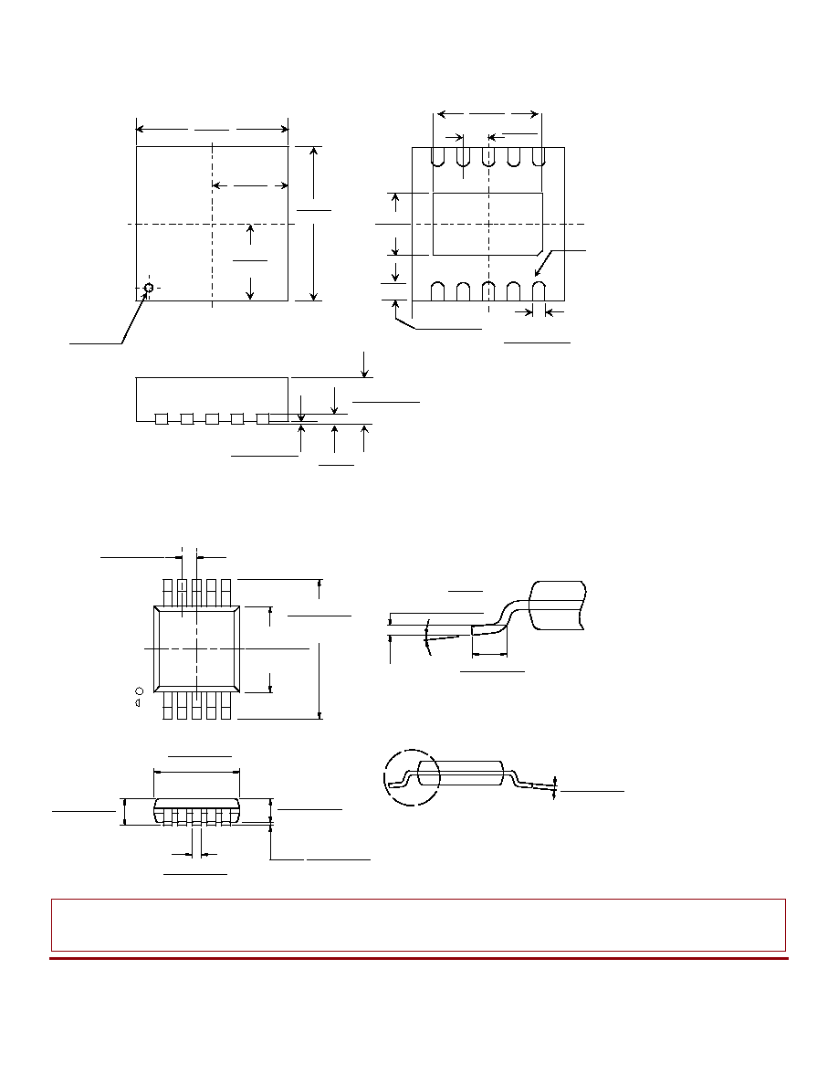
10-Lead DFN/MLP Package Outline (K6)
10-Lead MSOP Package Outline (MG)
Dimensions in Inches
(Dimensions in Millimeters)
Notes:
1. Measurement Legend =
2. MLP Package dimensions conform to JEDEC MO-229
0.010
(0.250)
DETAIL A
SEE DETAIL A
0∞≠ 6∞
GATE PLANE =
0.118±0.004
(3.000±0.100)
0.193±0.004
(4.900±0.100)
0.020±0.006
(0.500±0.152)
0.007±0.002
(0.180±0.050)
0.004±0.002
(0.100±0.050)
0.013±0.003
(0.325±0.075)
0.037±0.005
(0.950±.015)
0.118±0.004
(3.000±0.100)
0.021±0.005
(0.550±0.150)
0.033±0.004
(0.850±0.100)
*
*
Full Circle
or Half Circle
Pin #1 Index
Pin #1 Index
0.118
(3.000)
0.118
(3.000)
0.063
(1.600)
0.087
(2.200)
0.020
(0.500)
Bottom View
Top View
0.035±0.004
(0.900±0.100)
0.008
(0.200)
Side View
0.059
(1.500)
0.059
(1.500)
0.010
0.250
+0.002
-0.003
+0.050
-0.070
)
0.012
0.300
+0.006
-0.004
+0.150
-0.100
)
0.001
0.020
+0.001
-0.001
+0.030
-0.020
)
)
)
)