 | –≠–ª–µ–∫—Ç—Ä–æ–Ω–Ω—ã–π –∫–æ–º–ø–æ–Ω–µ–Ω—Ç: HV843 | –°–∫–∞—á–∞—Ç—å:  PDF PDF  ZIP ZIP |
1
HV843
Initial Release
Low Noise Dual EL Lamp Driver
Features
Low audible noise
Independent input control for lamp selection
180V
pp
output voltage
Split supply capability
Patented output timing
One miniature inductor to power both lamps
Low shutdown current
Wide input voltage range 2.0V to 5.8V
Output voltage regulation
No SCR output
Available in DFN/MLP - 10 package
Applications
Dual display cellular phones
Keypad and LCD backlighting
Portable instrumentation
Dual segment lamps
Hand held wireless communication devices
General Description
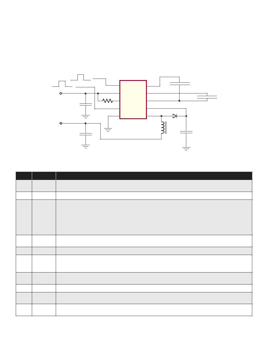
The Supertex HV843 is a low noise, high voltage driver designed
for driving two EL lamps with a combined area of 3.5 square
inches. The input supply voltage range is from 2.0V to 5.8V.
The device is designed to reduce the amount of audible noise
emitted by the lamp. This device uses a single inductor and a
minimum number of passive components to drive two EL lamps.
The nominal regulated output voltage of ±90V is applied to the
EL lamps. The two EL lamps can be turned ON and OFF by the
two logic input control pins, C
1
and C
2
. The device is disabled
when both C
1
and C
2
(pins 1 and 4) are at logic low.
The HV843 has an internal oscillator, a switching MOSFET, and
two high voltage EL lamp drivers. Each driver has its own half
bridge common output (COM1 and COM2) connected to a single
pin called COM which minimizes the DC offset seen by the EL
lamp. An external resistor connected between the R
SW-OSC
pin and
the voltage supply pin, V
DD
, sets the frequency for the switching
MOSFET. The EL lamp driver frequency is set by dividing the
MOSFET switching frequency by 512. An external inductor is
connected between the L
X
and the V
DD
pins. Depending on the EL
lamp size, a 1.0 to 10.0nF, 100V capacitor is connected between
C
S
and Ground. The switching MOSFET charges the external
inductor and discharges it into the capacitor at C
S
. The voltage
at C
S
increases. Once the voltage at C
S
reaches a nominal value
of 90V, the switching MOSFET is turned OFF to conserve power.
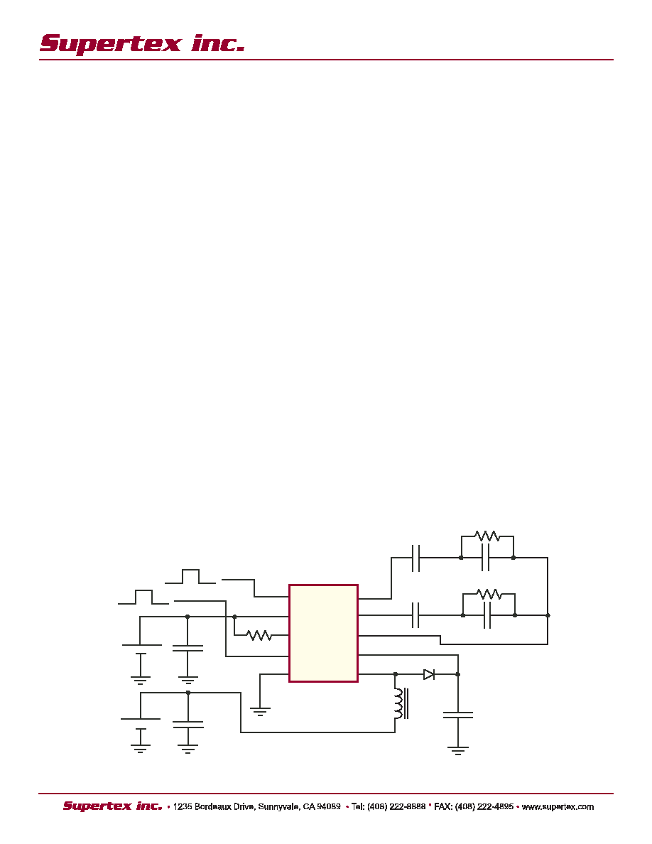
Typical Application Circuit
HV843K7-G
+
-
+
-
1
2
3
4
5
6
7
8
9
10
V
DD
Com
C
2
GND
EL
2
L
X
C
S
EL
1
C
1
R
SW-OSC
D
1.0µF
1.5V
0
1.5V
0
V
DD
V
IN
C
IN
4.7µF
C
DD
0.1µF
845k
3.3M
3.3M
EL Lamp 1
EL Lamp 2
1.0µF
L
X
330
µH
C
S
3.3nF, 100V
2
HV843
Ordering Information
Device
Package Options
DFN/MLP - 10
HV843
HV843K7-G
-G indicates package is RoHS compliant (`Green')
Absolute Maximum Ratings
Symbol
Parameter
Min
Typ
Max
Units
Conditions
Electrical Characteristics
(Over recommended operating conditions unless otherwise specifi ed - V
IN
= V
DD
= 3.3V, T
A
=25∞C)
Absolute Maximum Ratings are those values beyond which damage to the device may
occur. Functional operation under these conditions is not implied. Continuous operation
of the device at the absolute rating level may affect device reliability. All voltages are
referenced to device ground.
Parameter
Value
Supply Voltage, V
DD
-0.5V to 7.5V
Output Voltage, V
CS
-0.5V to 120V
Operating Temperature Range
-40∞C to 85∞C
Storage temperature
-65∞C to 150∞C
Symbol
Parameter
Min
Typ
Max
Units
Conditions
Recommended Operating Conditions
V
DD
Supply voltage
2.0
5.8
V
---
T
A
Operating temperature
-40
+85
o
C
---
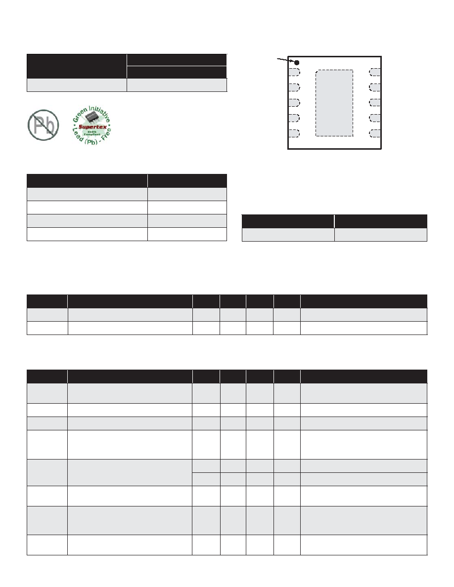
Pin Confi guration
Thermal Resistance
Package
ja
DFN/MLP - 10
60
o
C/W
Note: Mounted on FR4 board, 25mm x 25mm x 1.57mm
R
DS(ON)
On-resistance of switching
transistor
-
-
10
I = 100mA
V
DD
Input voltage range
2.0
-
5.8
V
---
V
CS
Output regulation voltage
80
90
100
V
V
DD
= 2.0V to 5.8V
V
DIFF
Differential output peak to peak
voltage
(EL
1
to COM, EL
2
to COM)
160
180
200
V
V
DD
= 2.0V to 5.8V
I
DDQ
Quiescent V
DD
supply current
-
-
150
nA
C
1
= C
2
= 0.1V
-
-
250
nA
C
1
= C
2
= 0.3V
I
DD
Input current into the V
DD
pin
-
-
250
A
V
DD
= 5.8V
I
IN
Average input current including
inductor current when driving both
lamps
-
20
30
mA
V
IN
= 5.5V (See Figure 1)
V
CS
Output voltage on V
CS
when driving
both lamps
-
87
-
V
V
IN
= 5.5V (See Figure 1)
HV843K7-G
Top View
C
1
V
DD
R
SW-OSC
C
2
GND
EL
1
EL
2
COM
C
S
L
X
Pin 1
Note: Pads are on the bottom of the package.
Back-side heat slug is at ground potential.
3
HV843
V
DIF
Differential output peak to peak
voltage across each lamp (EL
1
to
COM1, EL
2
to COM2)
160
180
200
V
V
IN
= 5.5V (See Figure 1)
f
EL
V
DIFF
output drive frequency
170
200
230
Hz
R
SW
= 845k
f
SW
Switching transistor frequency
87
102
118
kHz
R
SW
= 845k
f
SW temp
Switching transistor frequency
tempco
-
15
-
%
T
A
= -40∞C to +85∞C
D
Switching transistor duty cycle
-
85
-
%
T
A
= -40∞C to +85∞C
I
IL
Input logic low current
-
-
1.0
A
V
DD
= 2.0V to 5.8V
I
IH
Input logic low current
-
-
1.0
A
V
DD
= 2.0V to 5.8V
V
IL
Logic input low voltage
0
-
0.3
V
---
V
IH
Logic input high voltage
1.5
-
V
DD
V
---
Symbol
Parameter
Min
Typ
Max
Units
Conditions
Electrical Characteristics (cont.)
Functional Block Diagram
V
CS
Output
Drivers
V
SENSE
-
+
V
REF
Control logic
and switch
oscillator
Disable
Logic control and
divide by 512
EL
1
EL
2
R
SW-OSC
C
S
L
X
V
DD
C
1
C
2
GND
COM1
C
COM
COM2
V
DD
V
CS
V
CS
Function Table
Logic Inputs
Outputs
Device
C
1
C
2
EL
1
EL
2
COM
0
0
Hi Z
Hi Z
Hi Z
OFF
0
1
Hi Z
ON
ON
ON
1
0
ON
Hi Z
ON
ON
1
1
ON
ON
ON
ON
4
HV843
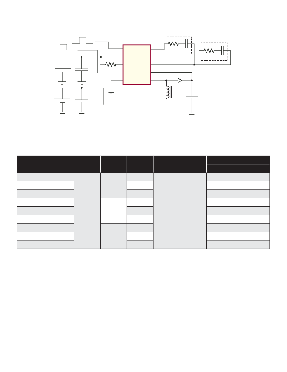
Figure 1 - Test Circuit
+
-
+
-
1
2
3
4
5
6
7
8
9
10
V
DD
Com
C
2
GND
EL
2
L
X
C
S
EL
1
C
1
R
SW-OSC
HV843K7-G
2.1in
2
EL Lamp 1***
1.8in
2
EL Lamp 2***
845k
C
DD
0.1µF
C
IN
4.7µF
V
IH
= ON
0 = OFF
V
IH
= ON
0 = OFF
V
DD
V
IN
620
13nF
620
11nF
1N4148*
C
S
3.3nF, 100V
L
X
330µH**
* or any (equivalent or better) > 90V, fast recovery diode
** Cooper LPO6610-334MLB
*** The bigger sized lamp should be tied to EL1 and the smaller
sized lamp to EL2 (pins 10 and 9 respectively)
Typical Performance
Lamp
V
DD
(V)
V
IN
(V)
I
IN
(mA)
V
CS
(V
PEAK
)
f
EL
(Hz)
Lamp Brightness (cd/m
2
)
EL
1
EL
2
EL
1
ON
3.0V
5.2V
7.96
88
195
13.89
-
EL
2
ON
6.91
-
12.89
Both EL
1
and EL
2
ON
13.93
13.02
11.24
EL
1
ON
5.5V
7.47
13.93
-
EL
2
ON
6.42
-
13.22
Both EL
1
and EL
2
ON
13.42
13.30
12.05
EL
1
ON
5.8V
7.04
14.03
-
EL
2
ON
6.01
-
13.30
Both EL
1
and EL
2
ON
12.94
13.55
12.51
5
HV843
Figure 2 - Split Supply Confi guration
HV843K7-G
1
2
3
4
5
6
7
8
9
10
V
DD
Com
C
2
GND
EL
2
L
X
C
S
EL
1
C
1
R
SW-OSC
D
C
S
L
X
C
IN
C
DD
V
IH
= ON
0 = OFF
V
IH
= ON
0 = OFF
Regulated Voltage = V
DD
Battery Voltage = V
IN
R
SW-OSC
EL Lamp 1
EL Lamp 2
Split Supply Confi guration
The HV843 can be used in applications operating from a
battery where a regulated voltage is available. This is shown
in Figure 2. The regulated voltage can be used to drive the
internal logic of HV843. The amount of current used to drive
the internal logic is less than 200µA. Therefore, the regu-
lated voltage could easily provide the current without being
loaded down.
Pin Confi guration and Description
Pin #
Function
Description
1
C
1
Enable input signal for EL Lamp 1. Logic high will turn ON the EL lamp 1 and logic low will turn it
OFF. Refer to the function table.
2
V
DD
Input voltage supply pin.
3
R
SW-OSC
External resistor connection to set both the switching MOSFET frequency and EL Lamp frequency.
The external resistor should be connected between V
DD
and this pin. The EL lamp frequency is the
switching frequency divided by 512. The switching frequency is inversely proportional to the resis-
tor value. A 845k resistor will provide a nominal switching frequency of 102kHz and an EL lamp
frequency of 200Hz. To change the frequency to f
EL1
, the value of the resistor R
SW-OSC1
can be deter-
mined as R
SW-OSC1
= (845 x 200) / f
EL1
k.
4
C
2
Enable input signal for EL Lamp 2. Logic high will turn ON the EL lamp 2 and logic low will turn it
OFF. Refer to the function table.
5
GND
Device ground.
6
L
X
Drain of internal switching MOSFET. Connection for an external inductor. When the switching
MOSFET is turned ON, the inductor is being charged. When the MOSFET is turned OFF, the energy
stored in the inductor is transferred to the high voltage capacitor connected at the C
S
pin.
7
C
S
Connect a 100V capacitor between this pin and GND. This capacitor stores the energy transferred
from the inductor.
8
COM
Common lamp connection for both EL
1
and EL
2
. Connect one end of both the lamps to this pin.
9
EL
2
EL lamp 2 connection. For optimum performance, the smaller of the two lamps should be connected
to this pin.
10
EL
1
EL lamp 1 connection. For optimum performance, the larger of the two lamps should be connected
to this pin.
6
Doc.# DSFP - HV843
062606
HV843
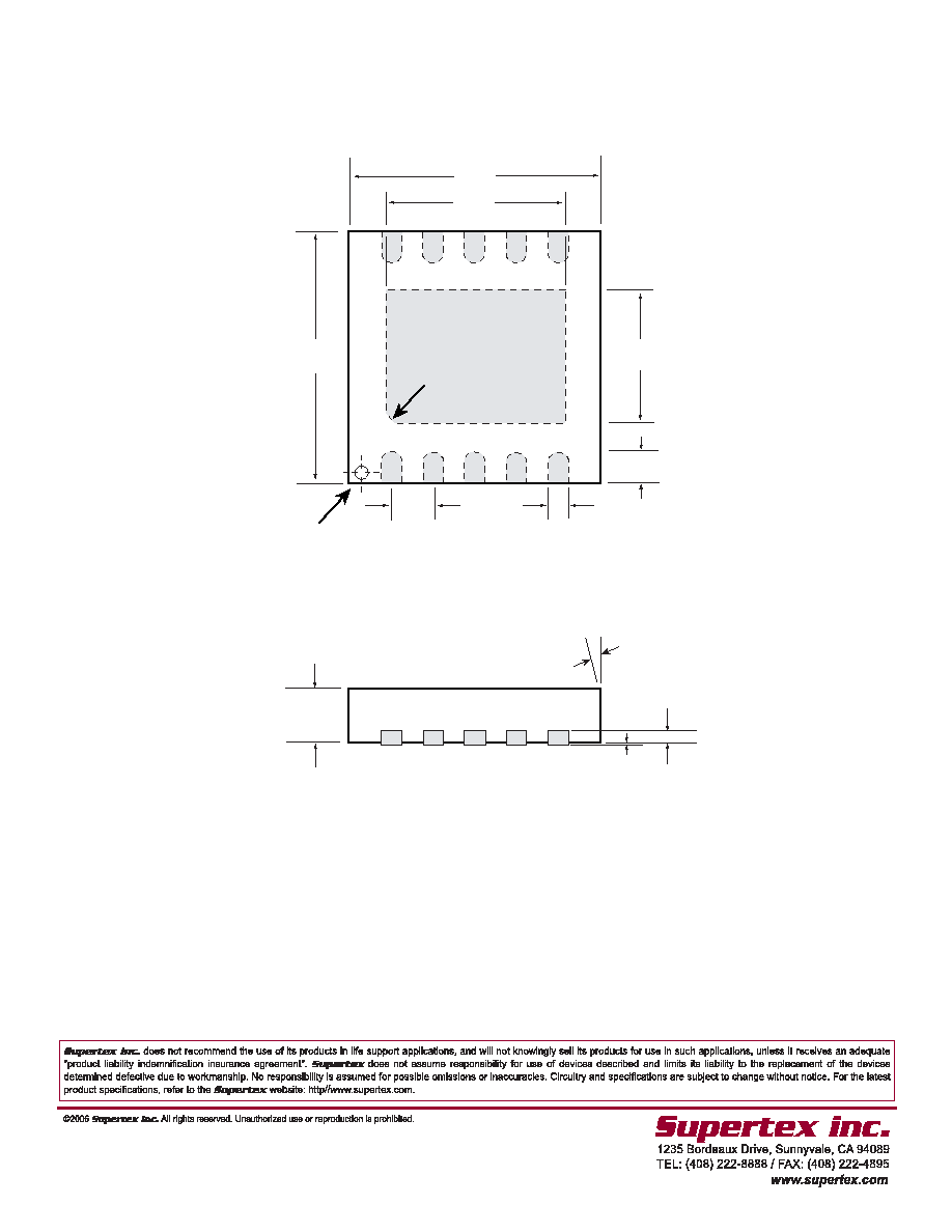
10-Lead DFN/MLP Package Outline (K7)
Top View
Side View
0.30
+0.15
-0.10
1.60
3.00
Note:
1. All dimensions are in millimeters; angles in degrees
2. Corner shape may differ from drawing
0.50 BSC
Pin #1 Index
3.00
2.20
0.20
0.25
+0.05
-0.07
0.0 - 0.05
0
O
- 14
O
Note 2
0.75 - 0.80