 | –≠–ª–µ–∫—Ç—Ä–æ–Ω–Ω—ã–π –∫–æ–º–ø–æ–Ω–µ–Ω—Ç: HV858MG-G | –°–∫–∞—á–∞—Ç—å:  PDF PDF  ZIP ZIP |

1
A011706
Tri-EL Lamp Driver IC
Features
Tri-EL lamp driver with common terminal
Independent brightness control for all 3 lamps
1.8V to 6.5V Operating Supply Voltage
Output voltage regulation
Two-pin serial data communication for control
Linear brightness control with seven steps at constant
effi
ciency
128kHz Fixed Switching Frequency
Split supply capability
Patented high effi ciency EL lamp driver
Single miniature inductor drives all 3 lamps
Only 4 external components
Burst mode power converter for best effi ciency
CMOS compatible serial interface with noise rejection
150nA max. leakage current when disabled
Power-on reset causes all outputs to be off when fi rst
powered
up
Small 10-pin MSOP package
10-pin DFN/MLP package (0.8mm thickness)
Applications
Mulit-segment, variable displays
Cell phone keypads and displays
MP3 players
Watches
General Description
The Supertex HV858 is a high voltage triple EL lamp driver
designed for driving combined EL lamps of up to 3.0 in
2
(1.0 in
2
each). The input supply voltage range is from 1.8V
to 6.5V. The device is designed such that the input voltage
to the inductor can be different from the input voltage to the
device (split supply). The device uses a single inductor and
a minimum number of passive components. The nominal
regulated output voltage that is applied to the EL lamp is
±95V. The HV858 has two internal oscillators, one for the
internal switching MOSFET, and the other for the high voltage
EL lamp driver. The EL lamp frequency is fi xed internally at
500Hz. The power converter oscillator runs 256 times faster
than the EL lamp driver at 128kHz.
An external inductor is connected between the L
X
and V
DD
pins (or between the L
X
pin and separate voltage source in
the case of a split supply application). A 0.002-0.01µF, 100V
capacitor is connected between the C
s
pin and ground.
The switching MOSFET charges the external inductor and
discharges it into the capacitor at the C
s
pin.
The voltage at
C
s
will start to increase. Once the voltage at C
s
reaches
a
nominal value of 95V, the switching MOSFET is turned OFF
to conserve power.
One side of the 3 EL lamps is connected to the Com pin of
HV858 and the other side to the EL1, EL2, and EL3 pins of the
HV858. Each EL lamp output may be independently controlled
to have one of the 7 brightness levels or can be completely
turned OFF by a 10-bit serial data input register. The 10-bit
control code has 3 bits to control the brightness level of each
EL Lamp and one bit to optionally control the power converter.
The 3-bit binary brightness control code controls the number
of 500Hz cycles (from 0 to 7) in a group of 7 cycles.
Typical Application Circuit
L
X
C
S
+
-
V
IN
D
+
-
V
DD
EL Lamp 1
7
8
9
10
6
EL Lamp 2
EL Lamp 3
HV858
C
IN
Clock
Serial Data in
C
DD
1
2
3
4
5
Com
EL2
C
S
EL1
EL3
V
DD
GND
L
X
SDI
SCK
Supertex inc.
HV858
Supertex inc.
∑
1235 Bordeaux Drive, Sunnyvale, CA 94089
∑
Tel: (408) 222-8888
∑
FAX: (408) 222-4895
∑
www.supertex.com
A011706
2
A011706
-40∫C to +85∫C
-65∫C to +150∫C
V
DD
-0.5 to +7V
SDI, SCK
I
SW
0.7A peak
V
CS
0.5 to +110V
Power dissipation
250mW
Storage temperature
Operating temperature
-0.5 to +7V
Absolute Maximum Ratings
Recommended Operating Conditions
Symbol
Parameter
Min
Typ
Max
Unit
Conditions
V
DD
Supply voltage
1.8
6.5
V
I
SW(pk)
Peak switch current
0.4
A
T
A
Operating temperature
-40
85
∫C
Specifi cations
(unless otherwise specifi ed: T
A
= 25∫C, V
DD
= 2.6V to 5.5V)
Symbol
Parameter
Min
Typ.
Max
Unit
Conditions
R
SW
ON resistance of switching transistor
4
6
V
DD
= 1.8 to 6.5V, I
SW
= 100mA
V
CS
Output voltage
85
95
105
V
S1...S9 = 0, V
DD
= 1.8 to 6.5V, no load
V
LAMP
Differential lamp voltage
170
190
210
V
COM
to any EL, no load, code
1
= 111
I
DD
V
DD
supply current
0.01
0.15
0.25
mA
V
CS
= 20V, no load, PWR_ON = 1
I
CS
V
CS
supply current
10
50
100
µ
V
CS
= 75V, no load
I
DDQ
V
DD
leakage current when disabled
100
150
nA
S1...S9 = 0, SCK and SDI can be tied to V
DD
or GROUND
f
SW
Inductor switching frequency
108.8
128
147.2
kHz
See Figure 1
425
500
575
For all codes except code
1
= 000
f
EL
Lamp frequency
Hz
V
LOW
Logic pin input Low level
-0.5
0
0.2 V
DD
V
V
HIGH
Logic pin input High level
V
DD
V
DD
+
0.5
V
I
LOGIC
Logic pin input current
-0.1
0
0.1
µ
0 < V
DD
< 7V
I
DD
Inductor current
56
70
mA
V
CS
Output voltage
82.5
V
f
EL
Lamp frequency
500
Hz
See Figure 1.
V
DD
= V
IN
= 3V, total lamp size = 3.0in
2
(1.0in
2
each), 10-bit SDI serial code = 1111111111
D
MAX
Maximum PWM switch duty cycle
80
88
94
%
V
CS
= 20V, R
LOAD
= 20
f
CLK
SCK speed
1
MHz
T
SU
SDI setup time before SCK rises
30
ns
T
H
SDI hold time before SCK rises
30
ns
0.8 V
DD
V
Note 1: Code refers to the 3-bit Brightness Control Code for the respective EL Lamp
Ordering Information
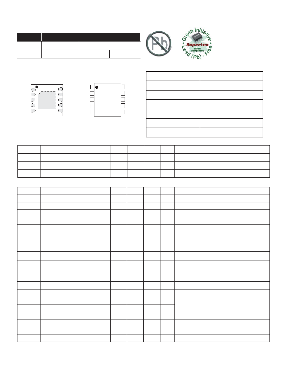
Pin Confi guration
Device
Package Options
HV858
DFN/MLP-10
MSOP-10
HV858K7-G
HV858MG
HV858MG-G
2
3
4
5
L
x
GND
SDI
EL3
2
3
4
5
MSOP-10
(top view)
DFN/MLP-10
(top view)
C
S
COM
SCK
1
1
7
8
9
6
V
DD
EL1
EL2
HV858MG
HV858K7
EL3
C
S
COM
EL1
EL2
L
x
GND
SDI
SCK
V
DD
7
8
9
10
6
10
-G indicates the package is RoHS compliant - "Green"
HV858
3
A011706
Pin Confi guration
Pin
Name Description
1
L
X
Inductor pin
2
GND
Ground pin
3
V
DD
Input voltage supply pin. It is common practice to use a bypass
capacitor as close as possible to the device on this pin.
4
SDI
Serial data input pin
5
SCK
Serial clock input pin
6
EL1
EL lamp 1 pin
7
EL2
EL lamp 2 pin
8
EL3
EL lamp 3 pin
9
COM
Common pin for one side of all 3 EL lamps
10
C
S
High Voltage capacitor pin
Logic Input Conditions
The serial data input consists of a 10-bit string, 3-bits of bright-
ness control and one bit(10
th
bit) to optionally control the power
converter. The power converter runs if any of the EL lamps has a
non-zero brightness value or if the PWR_ON bit is high while the
other 9 bits are low.
1. SDI may be H or L if SCK is H.
2. SCK may be H or L if SDI is H.
3. While inputting serial data to the shift register, SDI can
change value only when SCK is L.
4. The previous 10 bits of serial input will be latched when
SDI makes L to H transition while SCK is H.
EL Lamp Brightness Control
The EL Lamp brightness control is a 3-bit binary number stored
in a latch, which is provided by a serial to parallel conversion shift
register.
1.
If all the 3 bits for a designated EL lamp are L, the differential
voltage across that lamp will be zero.
2. If any of the 3 bits for a designated EL lamp is H:
a.
The 3-bit value sets the average number of cycles
for which the EL lamp voltage is non-zero.
b. The EL lamp brightness is linearly proportional
to the binary lamp control code.
Logic Input Diagram
S 1
S 2
S 3
S 4
S 5
S 6
S 7
S 8
S 9
S10
SDI
SCK
EL 1 Control
Latches
in Data
MSB of
EL1
LSB of
EL1
MSB of
EL2
LSB of
EL2
MSB of
EL3
LSB of
EL3
PWR_ON
EL 2 Control
EL 3 Control
Note:
1. Serial data is latched when SDI makes L to H transition and while SCK is H.
2. S1 is the fi rst serial data input being fed.
HV858
4
A011706
Logic Truth Table
L = Low (L = 0 to L < 20% of V
DD
)
H = High (80% of V
DD
< H = V
DD
)
NA = Does not control brightness of the designated EL lamp
Brightness
Level
S1
S2
S3
S4
S5
S6
S7
S8
S9
S10
Device
disabled
L
L
L
L
L
L
L
L
L
L
Device
enabled
All lamps
Off
L
L
L
L
L
L
L
L
L
H
7/7
H
H
H
NA
NA
NA
NA
NA
NA
NA
6/7
H
H
L
NA
NA
NA
NA
NA
NA
NA
5/7
H
L
H
NA
NA
NA
NA
NA
NA
NA
4/7
H
L
L
NA
NA
NA
NA
NA
NA
NA
3/7
L
H
H
NA
NA
NA
NA
NA
NA
NA
2/7
L
H
L
NA
NA
NA
NA
NA
NA
NA
1/7
L
L
H
NA
NA
NA
NA
NA
NA
NA
EL1
Off
L
L
L
NA
NA
NA
NA
NA
NA
NA
7/7
NA
NA
NA
H
H
H
NA
NA
NA
NA
6/7
NA
NA
NA
H
H
L
NA
NA
NA
NA
5/7
NA
NA
NA
H
L
H
NA
NA
NA
NA
4/7
NA
NA
NA
H
L
L
NA
NA
NA
NA
3/7
NA
NA
NA
L
H
H
NA
NA
NA
NA
2/7
NA
NA
NA
L
H
L
NA
NA
NA
NA
1/7
NA
NA
NA
L
L
H
NA
NA
NA
NA
EL2
Off
NA
NA
NA
L
L
L
NA
NA
NA
NA
7/7
NA
NA
NA
NA
NA
NA
H
H
H
NA
6/7
NA
NA
NA
NA
NA
NA
H
H
L
NA
5/7
NA
NA
NA
NA
NA
NA
H
L
H
NA
4/7
NA
NA
NA
NA
NA
NA
H
L
L
NA
3/7
NA
NA
NA
NA
NA
NA
L
H
H
NA
2/7
NA
NA
NA
NA
NA
NA
L
H
L
NA
1/7
NA
NA
NA
NA
NA
NA
L
L
H
NA
EL3
Off
NA
NA
NA
NA
NA
NA
L
L
L
NA
HV858
5
A011706
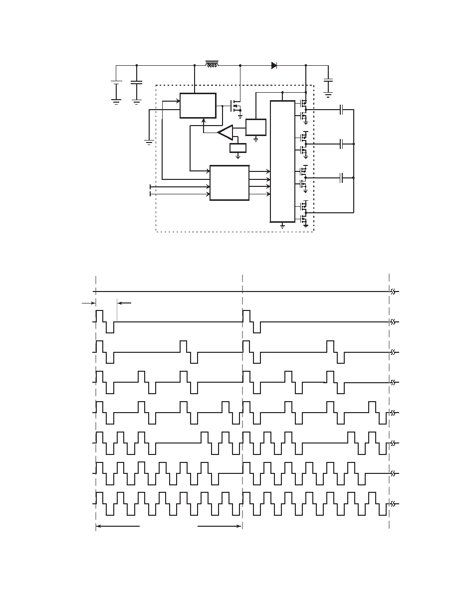
Vcs
EL2
Vcs
COM
Output
Drivers
V
SENSE
-
+
V
REF
Switch Osc
Disable
Logic Control
EL1
Vcs
EL3
Lx
1N914
Cs
Cs
L
X
V
DD
C
IN
GND
SDI
SCK
Enable
EL1
EL2
EL3
COM
+
-
V
IN
Note: This drawing is a generalized representation. Actual internal circuitry may differ.
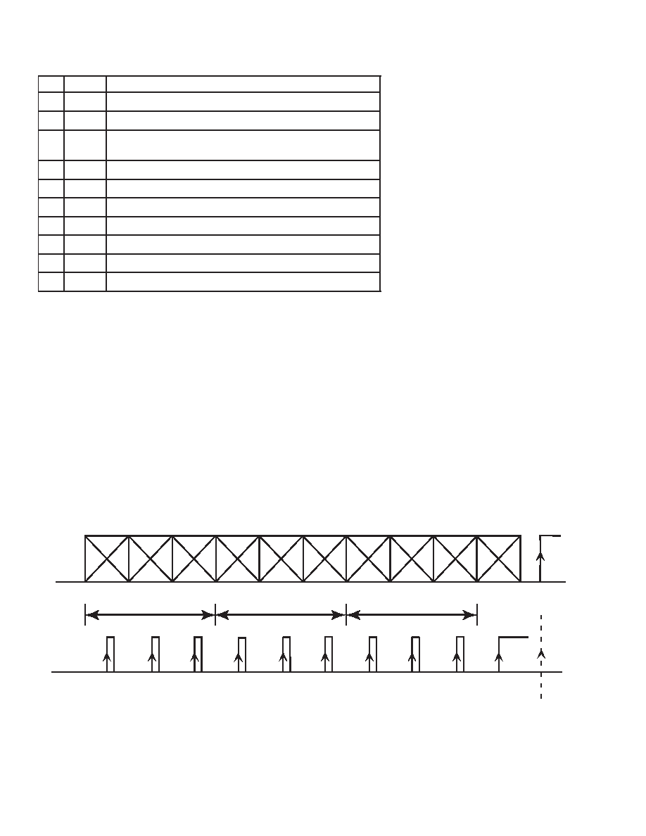
Differential Output Waveform
The following is the differential output waveform across the lamp for each 3-bit input code for each lamp.
Code 111
Code 110
Code 101
Code 100
Code 011
Code 010
Code 001
Code 000
Group of 7 Cycles
500Hz
.....Pattern Repeats....
Functional Block Diagram
HV858
6
A011706
*Any 100V fast reverse recovery diode can be used
Note: Maximum lamp size for each segment is 1.0 in
2
. To drive larger size lamps, any combination of EL1, EL2 and EL3 can be paralleled. However,
the 3-bit serial data input code (for each output) should be such that the paralleled outputs have the same code.
Com
EL2
L
X
= 68µH **
C
S
C
S
= 3.3nF, 100V
+
-
V
IN
D = IN914*
+
-
V
DD
EL1
7
8
9
10
EL3
6
EL Lamp 3
(1.0 in
2
)
HV858
C
IN
= 4.7µF
Stream of
Serial Data
(1's and 0's)
C
DD
=
0.1µF
V
DD
GND
1
2
3
4
L
X
SDI
SCK
5
EL Lamp 2
(1.0 in
2
)
EL Lamp 1
(1.0 in
2
)
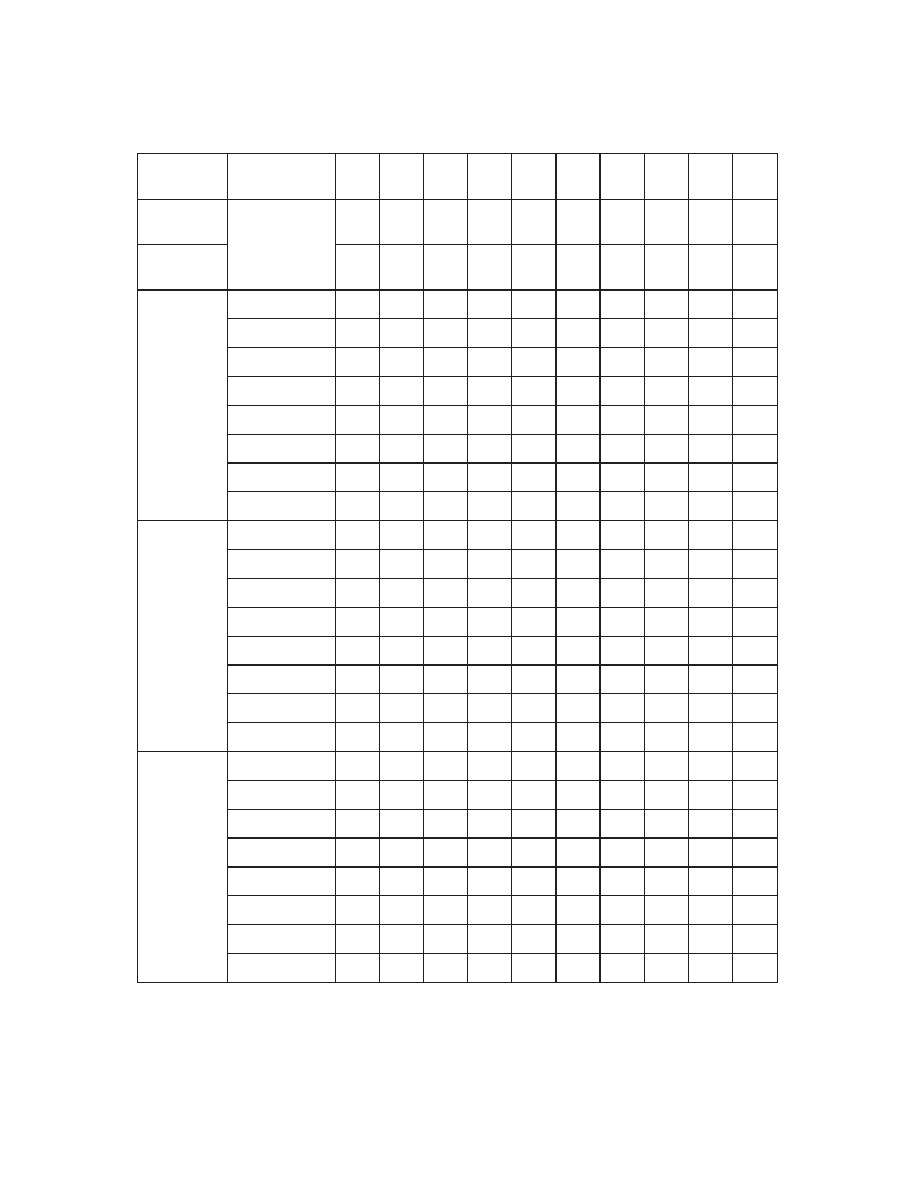
Typical Performance
(V
DD
= V
IN
= 3.0V)
EL1 Brightness
1
st
9-bit SDI code
Level ft-lm Cd/m
2
I
DD
(mA)
V
CS
(V)
000111111 0/7
0 0 42.6
85.7
001111111 1/7
1.60
5.46
44.7
85.3
010111111 2/7
3.24
11.08
46.9
84.9
011111111 3/7
4.95
16.94
48.9
84.5
100111111 4/7
6.68
22.85
51.2
84.0
101111111 5/7
8.44
28.85
53.3
83.5
110111111 6/7
10.21
34.93
55.0
82.9
111111111 7/7
12.05
41.2
56.2
82.5
Figure 1 : Test Circuit
HV858
7
A011706
Supertex inc.
1235 Bordeaux Drive, Sunnyvale, CA 94089
TEL: (408) 222-8888 / FAX: (408) 222-4895
www.supertex.com
©2006 Supertex inc. All rights reserved. Unauthorized use or reproduction is prohibited.
Supertex inc.
does not recommend the use of its products in life support applications, and will not knowingly sell its products for use in such applications, unless it receives an adequate
"product liability indemnification insurance agreement". Supertex does not assume responsibility for use of devices described and limits its liability to the replacement of the devices
determined defective due to workmanship. No responsibility is assumed for possible omissions or inaccuracies. Circuitry and specifications are subject to change without notice. For the latest
product specifications, refer to the Supertex website: http//www.supertex.com.
Doc. # DSFP-HV858
A1011706
HV858
0.010
(0.250)
DETAIL A
SEE DETAIL A
0∞≠ 6∞
GATE PLANE =
0.118±0.004
(3.000±0.100)
0.193±0.004
(4.900±0.100)
0.020±0.006
(0.500±0.152)
0.007±0.002
(0.180±0.050)
0.004±0.002
(0.100±0.050)
0.013±0.003
(0.325±0.075)
0.037±0.005
(0.950±.015)
0.118±0.004
(3.000±0.100)
0.021±0.005
(0.550±0.150)
0.033±0.004
(0.850±0.100)
Full Circle
or Half Circle
10-Lead MSOP Package Outline (MG)
10-Lead DFN/MLP Package Outline (K7)
Pin #1 Index
Pin #1 Index
0.118
(3.000)
0.118
(3.000)
0.063
(1.600)
0.087
(2.200)
0.020
(0.500)
Bottom View
Top View
0.0295±0.002
(0.75±0.05)
0.008
(0.200)
Side View
0.059
(1.500)
0.059
(1.500)
0.010
0.250
+0.002
-0.003
+0.050
-0.070
)
0.012
0.300
+0.006
-0.004
+0.150
-0.100
)
0.001
0.020
+0.001
-0.001
+0.030
-0.020
)
)
)
)
Dimensions in Inches
(Dimensions in Millimeters)
1. Measurement Legend =
2. MLP Package dimensions conform to JEDEC MO-229