 | –≠–ª–µ–∫—Ç—Ä–æ–Ω–Ω—ã–π –∫–æ–º–ø–æ–Ω–µ–Ω—Ç: HV860K7-G | –°–∫–∞—á–∞—Ç—å:  PDF PDF  ZIP ZIP |
Supertex inc.
Supertex inc.
∑
1235 Bordeaux Drive, Sunnyvale, CA 94089
∑
Tel: (408) 222-8888
∑
FAX: (408) 222-4895
∑
www.supertex.com
1
NR040306
HV860
Initial Release
Features
Adjustable output regulation for dimming
220V
PP
output voltage for higher brightness
Single cell lithium ion compatible
150nA shutdown current
Separately adjustable lamp and converter frequencies
3x3 QFN-12 package
Split supply capability
Applications
Mobile cellular phone keypads
PDAs
Handheld wireless communication products
Global Positioning Systems (GPS)
The HV860 has two internal oscillators, a switching
MOSFET, and a high voltage EL lamp driver H-bridge. The
frequency for the switching MOSFET is set by an external
resistor connected between the R
SW-OSC
pin and the supply
pin V
DD
. The EL lamp driver frequency is set by an external
resistor connected between R
EL-OSC
pin and V
DD
pin. An
external inductor is connected between the L
X
and V
DD
pins or V
IN
for split supply applications. A 3.0nF capacitor
is connected between C
S
and ground. The EL lamp is
connected between V
A
and V
B
.
The switching MOSFET charges the external inductor and
discharges it into the capacitor at C
S
. The voltage at C
S
will
start to increase. Once the voltage at C
S
reaches a nominal
value of 110V, the switching MOSFET is turned OFF to
conserve power. The outputs V
A
and V
B
are confi gured as
an H bridge and are switching in opposite states to achieve
±110V across the EL lamp.
EL lamp dimming can be accomplished by changing the
input voltage to the V
REG
pin. The V
REG
pin allows an external
voltage source to control the V
CS
amplitude. The V
CS
voltage
is approximately 87 times the voltage seen on V
REG
.
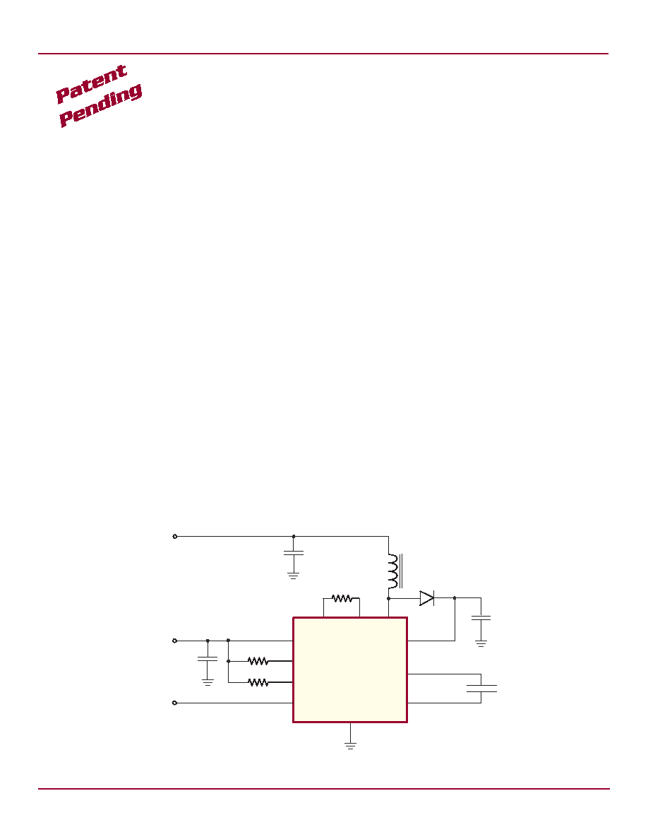
Typical Application Circuit
Low Noise Dimmable EL Lamp Driver
General Description
The Supertex HV860 is a high voltage driver designed for
driving Electroluminescent, (EL), lamps of up to 5 square
inches. The input supply voltage range is from 2.5V to 4.5V.
The device uses a single inductor and a minimum number of
passive components. Using the internal reference voltage,
the regulated output voltage is at a nominal voltage of 110V.
The EL lamp will therefore see ±110V. An enable pin, (EN),
is available to turn the device on and off via a logic signal.
V
DD
V
B
V
A
C
S
L
X
V
REF
V
REG
R
EL-OSC
R
SW-OSC
EN
GND
HV860K7
V
IN
1.5V = On
0V = Off
V
DD
EL
Lamp
C
S
C
DD
R
SW
R
EL
C
IN
L
X
D
R
REG
9
7
5
3
2
10
12
1
11
4
8

2
NR040306
HV860
Ordering Information
Device
Package Option
QFN-12
HV860
HV860K7-G
-G indicates package is RoHS compliant (`Green')
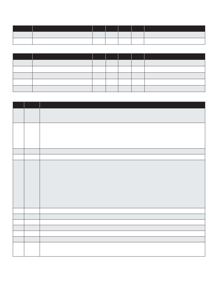
Absolute Maximum Ratings
Parameter
Value
V
DD
, Supply Voltage
-0.5V to 6.0V
Operating Temperature
-40∞C to +85∞C
Storage Temperature
-65∞C to +150∞C
Power Dissipation QFN-12
1.6W
V
CS
, Output Voltage
-0.5V to +120V
V
REG
External Input Voltage
1.33V
Symbol
Parameter
Min
Typ
Max
Units
Conditions
Electrical Characteristics
DC Characteristics
(Over recommended operating conditions unless otherwise specifi ed T
A
=25∞C)
Absolute Maximum Ratings are those values beyond which damage to the device may
occur. Functional operation under these conditions is not implied. Continuous operation
of the device at the absolute rating level may affect device reliability. All voltages are
referenced to device ground.
Pin Confi guration
Package
ja
QFN-12
60 ∞C/W
Thermal Resistance
R
DS(ON)
On-resistance of switching
transistor
-
-
6.0
I = 100mA
V
CS
Maximum output regulation voltage
-
-
120
V
V
DD
= 2.5V to 4.5V
V
CS
Output regulation voltage
-
95
-
V
V
DD
= 2.5V to 4.5V, V
REG
= 1.092V
-
75
-
V
DD
= 2.5V to 4.5V, V
REG
= 0.862V
-
55
-
V
DD
= 2.5V to 4.5V, V
REG
= 0.632V
V
REG
External input voltage range
0
-
1.26
V
V
DD
= 2.5V to 4.5V
V
REFH
V
REF
output high voltage
1.18
1.26
1.33
V
V
DD
= 2.5V to 4.5V
I
DDQ
Quiescent V
DD
supply current
-
-
150
nA
EN = low
I
DD
Input current going into the V
DD
pin
-
-
200
µA
V
DD
= 2.5V to 4.5V, R
EL
= 2.0M
,
R
SW
= 1.0M
I
IN
Input current including inductor
current
-
-
16
mA
see Figure 2
f
EL
EL lamp frequency
160
200
240
Hz
R
EL
= 2.0M
f
SW
Switching transistor frequency
76
90
104
kHz
R
SW
= 1.0M
D
Switching transistor duty cycle
-
-
88
%
---
V
IH
Enable input logic high voltage
1.5
-
V
DD
V
V
DD
= 2.5V to 4.5V
V
IL
Enable input logic low voltage
0
-
0.2
V
V
DD
= 2.5V to 4.5V
I
IH
Enable input logic high current
-
-
1.0
µA
V
IH
= V
DD
= 2.5V to 4.5V
1
2
3
4
5
6
7
8
9
10
11
12
HV860K7
GND L
X
C
S
V
B
V
A
V
DD
EN
V
REG
V
REF
R
EL-OSC
NC
R
SW-OSC
QFN-12 Top View
Note: Pads are at the bottom of the package. Center heat slug is at ground
potential
3
NR040306
HV860
Symbol
Parameter
Min
Typ
Max
Units
Conditions
Electrical Characteristics (cont.)
I
IL
Enable input logic low current
-
-
-1.0
µA
V
IL
= 0V, V
DD
= 2.5V to 4.5V
C
IN
Enable input capacitance
-
-
15
pF
---
Recommended Operating Conditions
Symbol
Parameter
Min
Typ
Max
Units
Conditions
V
DD
Supply voltage
2.5
-
4.5
V
---
f
SW
Switching frequency
40
-
200
kHz
---
f
EL
EL output frequency
200
-
500
Hz
---
C
LOAD
EL lamp capacitance load
0
-
20
nF
---
T
A
Operating Temperature
-40
-
+85
∞C
---
Pin Confi guration and External Component Description
Pin #
Name
Description
1
R
EL-OSC
External resistor from R
EL-OSC
to V
DD
sets the EL frequency. The EL frequency is inversely proportional
to the external R
EL
resistor value. Reducing the resistor value by a factor of two will result in increasing
the EL frequency by two.
2
V
REG
Input voltage to set V
CS
regulation voltage. This pin allows an external voltage source to control the V
CS
amplitude. EL lamp dimming can be accomplished by varying the input voltage to V
REG
. The V
CS
voltage
is approximately 87 times the voltage seen on V
REG
.
External resistor R
REG
, connected between V
REG
and V
REF
pins controlls the V
CS
charging rate. The
charging rate is inversely proportional to the R
REG
resistor value.
3
V
REF
Switched internal reference voltage.
4
GND
Device ground.
5
L
X
Drain of internal switching MOSFET. Connection for an external inductor.
The inductor L
X
is used to boost the low input voltage by inductive fl yback. When the internal switch
is on, the inductor is being charged. When the internal switch is off, the charge stored in the inductor
will be transferred to the high voltage capacitor C
S
. The energy stored in the capacitor is connected
to the internal H-bridge, and therefore to the EL lamp. In general, smaller value inductors, which can
handle more current, are more suitable to drive larger size lamps. As the inductor value decreases, the
switching frequency of the inductor (controlled by R
SW
) should be increased to avoid saturation.
A 220µH Cooper (SD3814-221) inductor with 5.5 series DC resistance is typically recommended. For
inductors with the same inductance value, but with lower series DC resistance, lower R
SW
resistor value
is needed to prevent high current draw and inductor saturation.
6
NC
No internal connections to the device.
7
C
S
High voltage regulated output. Connection for an external high voltage capacitor to ground
8
V
B
V
B
side of the EL lamp driver H-bridge. Connection for one of the EL lamp terminals.
9
V
A
V
A
side of the EL lamp driver H-bridge. Connection for one of the EL lamp terminals.
10
V
DD
Low voltage input supply pin.
11
EN
Logic input pin. Logic high will enable the device.
12
R
SW-OSC
External resistor from R
SW-OSC
to V
DD
sets the switch converter frequency. The switch converter frequency
is inversely proportional to the external R
SW
resistor value. Reducing the resistor value by a factor of two
will result in increasing the switch converter frequency by two.
4
NR040306
HV860
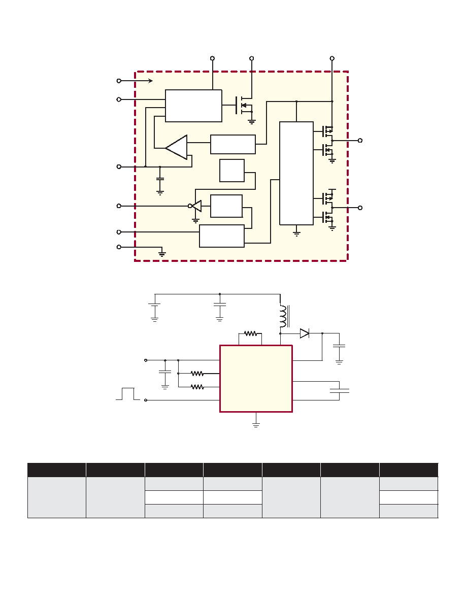
Figure 1: Block Diagram
V
A
V
B
V
CS
Output
Drivers
EL
Frequency
2x EL
Freq.
1.26V
V
REF
V
SENSE
PWM Switch
Oscillator
0 to 88%
Device Enable
EN
R
SW-OSC
V
REG
V
REF
R
EL-OSC
GND
60pF
V
DD
L
X
C
S
-
+
C
V
DD
V
B
V
A
C
S
L
X
V
REF
V
REG
R
EL-OSC
R
SW-OSC
EN
GND
HV860K7
V
IN
1.5V = ON
0V = Off
V
DD
3.0in
2
EL Lamp
3.3nF
200V
0.1F
1.0M
4.7F
BAS21
+
-
2.0M
3.3M
220H
(Cooper Inductor SD3814-221)
9
7
5
3
2
10
12
1
11
4
8
Figure 2: Typical Application / Test Circuit
V
DD
Lamp Size
V
IN
I
IN
V
CS
f
EL
Brightness
3.0V
3.0in
2
3.0V
16.17mA
100V (peak)
196Hz
18.2cd/m
2
3.5V
14.18mA
19.3cd/m
2
4.2V
12.13mA
19.9cd/m
2
Typical Performance

5
NR040306
HV860
Split Supply Confi guration
Enable/Disable Confi guration
The HV860 can also be used for handheld devices operating
from a battery where a regulated voltage is available. This
is shown in the Figure 4. The regulated voltage can be used
to run the internal logic of the HV860. The amount of current
necessary to run the internal logic is 200µA max. Therefore,
the regulated voltage could easily provide the current without
being loaded down.
The HV860 can be easily enabled and disabled via a logic
control signal on the EN pin as shown in the Figure 4. The
control signal can be from a microprocessor. When the
microprocessor signal is high the device is enabled, and
when the signal is low, it is disabled.
Figure 4: Split Supply and Enable/Disable Confi guration
V
DD
V
B
V
A
C
S
L
X
V
REF
V
REG
R
EL-OSC
R
SW-OSC
EN
GND
HV860K7
V
IN
Regulated Voltage = V
DD
EL
Lamp
C
S
R
SW
R
EL
C
IN
L
X
D
R
REG
+
-
9
7
5
3
2
10
12
1
11
4
8
On = 1.5V
Off = 0V
C
DD
Figure 3: Typical Waveform on V
A
, V
B
, and Differential Waveform V
A
- V
B

6
NR040306
HV860
Figure 5: Typical Application Circuit for Audible Noise Reduction
V
DD
V
B
V
A
C
S
L
X
V
REF
V
REG
R
EL-OSC
R
SW-OSC
EN
GND
HV860K7
V
IN
1.5V = On
0V = Off
V
DD
EL
Lamp
C
S
C
DD
R
SW
R
EL
C
IN
L
X
D
R
REG
9
7
5
3
2
10
12
1
11
4
8
The EL lamp, when lit, emits an audible noise. This is due
to EL lamp construction. The audible noise generated by the
EL lamp can be a major problem for applications where the
EL lamp is held close to the ear, such as cellular phones.
The HV860 employs a proprietary circuit to help minimize
the EL lamp's audible noise by using a single resistor, R
REG
,
as shown in Figure 5.
Audible Noise Reduction
The audible noise from the EL lamp can be minimized with
the proper selection of R
REG
. R
REG
is connected between
the V
REF
and V
REG
pins. V
REG
has an internal 60pF capacitor
to ground. EL lamp noise can be minimized without much
loss in brightness by setting the RC time constant to be
approximately 1/12
TH
of the EL frequency's period.
Figure 6: PWM Dimming Circuit
V
DD
V
B
V
A
C
S
L
X
V
REF
V
REG
R
EL-OSC
R
SW-OSC
EN
GND
HV860K7
V
IN
V
DD
EL Lamp
3.3nF
200V
0.1F
1.0M
4.7F
BAS21
2.0M
3.3M
220H
(Cooper Inductor SD3814-221)
9
7
5
3
2
10
12
1
11
4
8
10k
Open Drain
n-channel
PWM Signal
+
-
On = 1.5V
Off = 0V
+
-
How to Minimize EL Lamp Audible Noise
This section describes the method of dimming the EL lamp.
Reducing the voltage amplitude at the V
REG
pin will reduce
the voltage on the V
CS
pin, which will effectively reduce the
peak the peak voltage the EL lamp sees. Figure 5 shows a
circuit to dim the lamp by changing the duty cycle of a PWM
signal. A 10k resistor is connected in series with a 3.3M
resistor. An n-channel open drain PWM signal is used to pull
the 10k resistor to ground. The effective voltage on the
V
REG
pin will be proportional to the duty cycle of the PWM
signal. The PWM operating frequency can be anywhere
between 20kHz to 100kHz.
EL Lamp Dimming using PWM
Supertex inc.
1235 Bordeaux Drive, Sunnyvale, CA 94089
TEL: (408) 222-8888 / FAX: (408) 222-4895
www.supertex.com
©2006 Supertex inc. All rights reserved. Unauthorized use or reproduction is prohibited.
Supertex inc.
does not recommend the use of its products in life support applications, and will not knowingly sell its products for use in such applications, unless it receives an adequate
"product liability indemnification insurance agreement". Supertex does not assume responsibility for use of devices described and limits its liability to the replacement of the devices
determined defective due to workmanship. No responsibility is assumed for possible omissions or inaccuracies. Circuitry and specifications are subject to change without notice. For the latest
product specifications, refer to the Supertex website: http//www.supertex.com.
7
Doc.# DSFP - HV860
NR040306
HV860
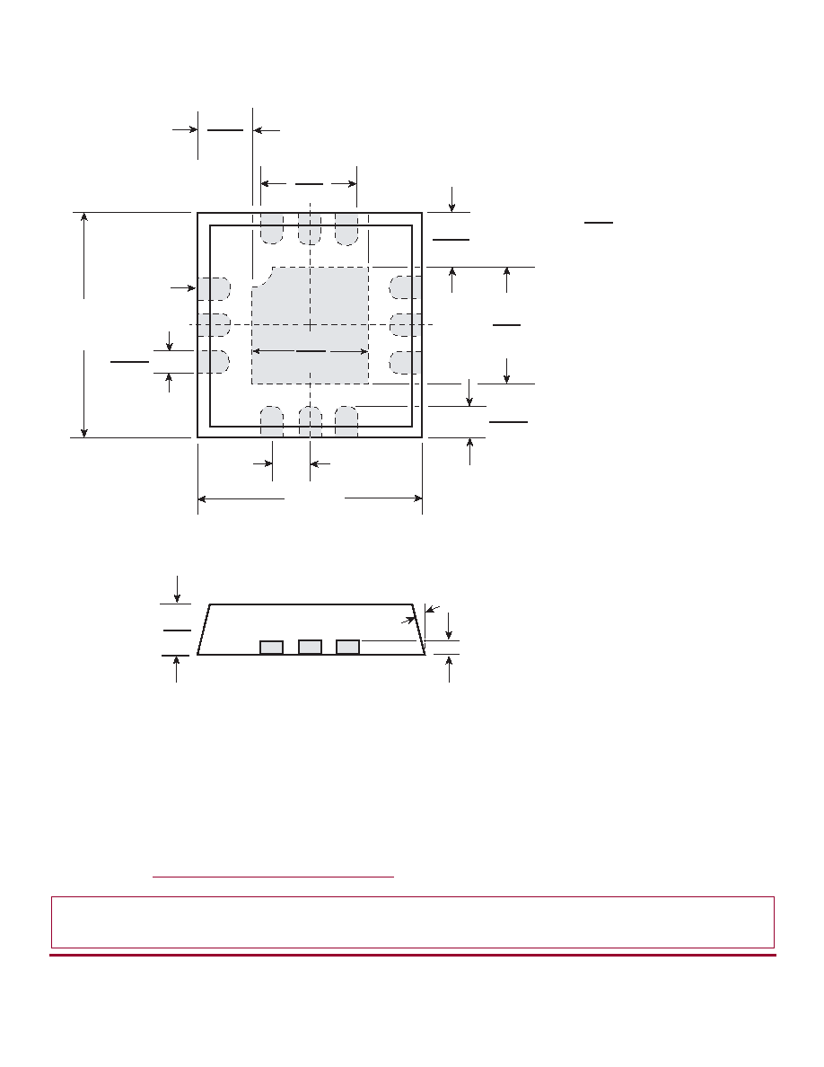
12-Lead QFN Package Outline (K7)
Top View
Side View
3.00
3.00
Pin #1
All dimensions are in millimeters
Legend: min
max
1.55
2.40
0.30
0.50
0.70
0.80
1.25
1.65
0.73
0.85
1.25
1.65
0.5
0.73
0.85
0.20
0.18
0.30
~ 14
O
(The package drawing(s) in this data sheet may not refl ect the most current specifi cations. For the latest package outline
information go to
http://www.supertex.com/packaging.html
.)