1
Ordering Information
Device
Recommended
44 J-Lead
Dice in
Operating
Quad Plastic
Waffle Pack
V
PP
max
Chip Carrier
Chip Carrier
HV9308
80V
HV9308PJ
HV9308X
HV9408
80V
HV9408PJ
HV9408X
Features
Processed with HVCMOS
Æ
technology
Low power level shifting
Shift register speed 8MHz
Latched data outputs
5V CMOS compatible inputs
Forward and reverse shifting options
Diode to V
PP
allows efficient power recovery
44-lead ceramic surface mount package
Hi-Rel processing available
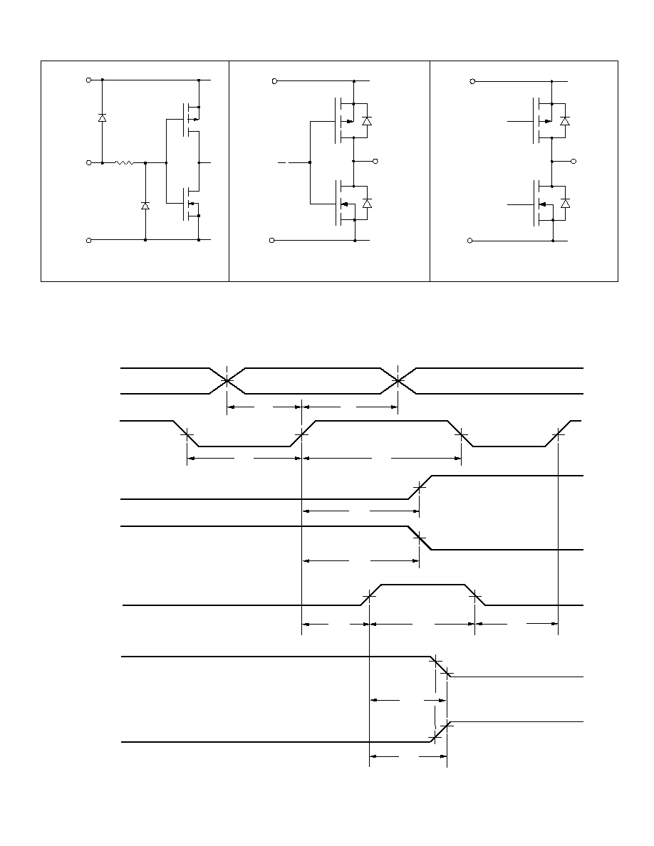
General Description
The HV93 and HV94 are low voltage serial to high voltage parallel
converters with push-pull outputs. These devices have been
designed for use as drivers for AC-electroluminescent displays.
They can also be used in any application requiring multiple output
high voltage current sourcing and sinking capabilities such as
driving plasma panels, vacuum fluorescent, or large matrix LCD
displays.
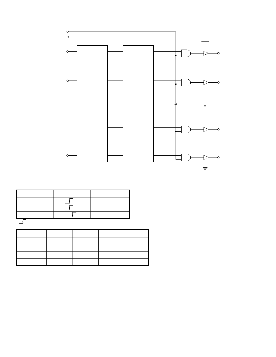
These devices consist of a 32-bit shift register, 32 latches, and
control logic to enable outputs. HV
OUT
1 is connected to the first
stage of the shift register through the Output Enable logic. Data is
shifted through the shift register on the low to high transition of the
clock. The HV94 shifts in the counterclockwise direction when
viewed from the top of the package and the HV93 shifts in the
clockwise direction. A data output buffer is provided for cascading
devices. This output reflects the current status of the last bit of the
shift register (32). Operation of the shift register is not affected by
the LE (latch enable) or the OE (output enable) inputs. Transfer
of data from the shift register to the latch occurs when the LE input
is high. The data in the latch is retained when LE is low.
Absolute Maximum Ratings
1
Supply voltage, V
DD
2
-0.5V to +7V
Supply voltage, V
PP
2
-0.5V to +90V
Logic input levels
2
-0.5 to V
DD
+ 0.5V
Ground current
3
1.5A
Continuous total power dissipation
4
1200mW
Operating temperature range
-40
∞
C to 85
∞
C
Storage temperature range
-65
∞
C to +150
∞
C
Lead temperature 1.6mm (1/16 inch)
260
∞
C
from case for 10 seconds
Notes:
1. Device will survive (but operation may not be specified or guaranteed) at
these extremes.
2. All voltages are referenced to GND
1
.
3. Duty cycle is limited by the total power dissipated in the package.
4. For operation above 25
∞
C ambient derate linearly to maximum operating
temperature at 20mW/
∞
C.
HV9308
HV9408
32-Channel Serial To Parallel Converter
With High Voltage Push-Pull Outputs
Package Options
02/96/022
Supertex Inc. does not recommend the use of its products in life support applications and will not knowingly sell its products for use in such applications unless it receives an adequate "products liability
indemnification insurance agreement." Supertex does not assume responsibility for use of devices described and limits its liability to the replacement of devices determined to be defective due to
workmanship. No responsibility is assumed for possible omissions or inaccuracies. Circuitry and specifications are subject to change without notice. For the latest product specifications, refer to the
Supertex website: http://www.supertex.com. For complete liability information on all Supertex products, refer to the most current databook or to the Legal/Disclaimer page on the Supertex website.
2
HV9308/HV9408
Recommended Operating Conditions
Symbol
Parameter
Min
Max
Units
V
DD
Logic Voltage Supply
4.5
5.5
V
V
PP
High Voltage Supply
8.0
80
V
V
IH
Input HIGH Voltage
V
DD
-0.5
V
DD
V
V
IL
Input LOW Voltage
0
0.5
V
f
CLK
Clock Frequency
0
8.0
MHz
T
A
Operating Free-Air Temperature
Plastic
-40
+85
∞
C
Ceramic
-55
+125
∞
C
Notes:
Power-up sequence should be the following:
1. Connect ground.
2. Apply V
DD
.
3. Set all inputs (Data, CLK, Enable, etc.) to a known state.
4. Apply V
PP
.
Power-down sequence should be the reverse of the above.
The V
PP
should not drop below V
DD
during operations.
Electrical Characteristics
(V
PP
= 60V, V
DD
= 5V, T
A
=25
∞
C)
DC Characteristics
Symbol
Parameter
Min
Max
Units
Conditions
I
PP
V
PP
Supply Current
100
µ
A
HV
OUT
outputs HIGH to LOW
I
DDQ
I
DD
Supply Current (Quiescent)
100
µ
A
All inputs = V
DD
or GND
I
DD
I
DD
Supply Current (Operating)
15
mA
V
DD
= V
DD
max,
f
CLK
= 8 MHz
V
OH
(Data)
Shift Register Output Voltage
V
DD
-0.5
V
I
O
= -100
µ
A
V
OL
(Data)
Shift Register Output Voltage
0.5
V
I
O
= 100
µ
A
I
IH
Current Leakage, any input
1.0
µ
A
Input = V
DD
I
IL
Current Leakage, any input
-1.0
µ
A
Input = GND
V
OC
HV
OUT
Output Clamp Diode Voltage
-1.5
V
I
OC
= -5mA
V
OH
HV
OUT
Output when Sourcing
52
V
I
OH
= -20mA, 0 to 70
∞
C
V
OL
HV
OUT
Output when Sinking
4.0
V
I
OL
= 5mA, 0 to 70
∞
C
AC Characteristics
Symbol
Parameter
Min
Max
Units
Conditions
f
CLK
Clock Frequency
8.0
MHz
t
WL
or t
WH
Clock width, HIGH or LOW
62
ns
t
SU
Setup time before CLK rises
25
ns
t
H
Hold time after CLK rises
10
ns
t
DLH
(Data)
Data Output Delay after L to H CLK
110
ns
C
L
= 15pF
t
DHL
(Data)
Data Output Delay after H to L CLK
110
ns
C
L
= 15pF
t
DLE
LE Delay after L to H CLK
50
ns
t
WLE
Width of LE Pulse
50
ns
t
SLE
LE Setup Time before L to H CLK
50
ns
t
ON
Delay from LE to HV
OUT
, L to H
500
ns
t
OFF
Delay from LE to HV
OUT
, H to L
500
ns
5
1235 Bordeaux Drive, Sunnyvale, CA 94089
TEL: (408) 744-0100 ∑ FAX: (408) 222-4895
www.supertex.com
02/06//02
©2002 Supertex Inc. All rights reserved. Unauthorized use or reproduction prohibited.
HV9308/HV9408
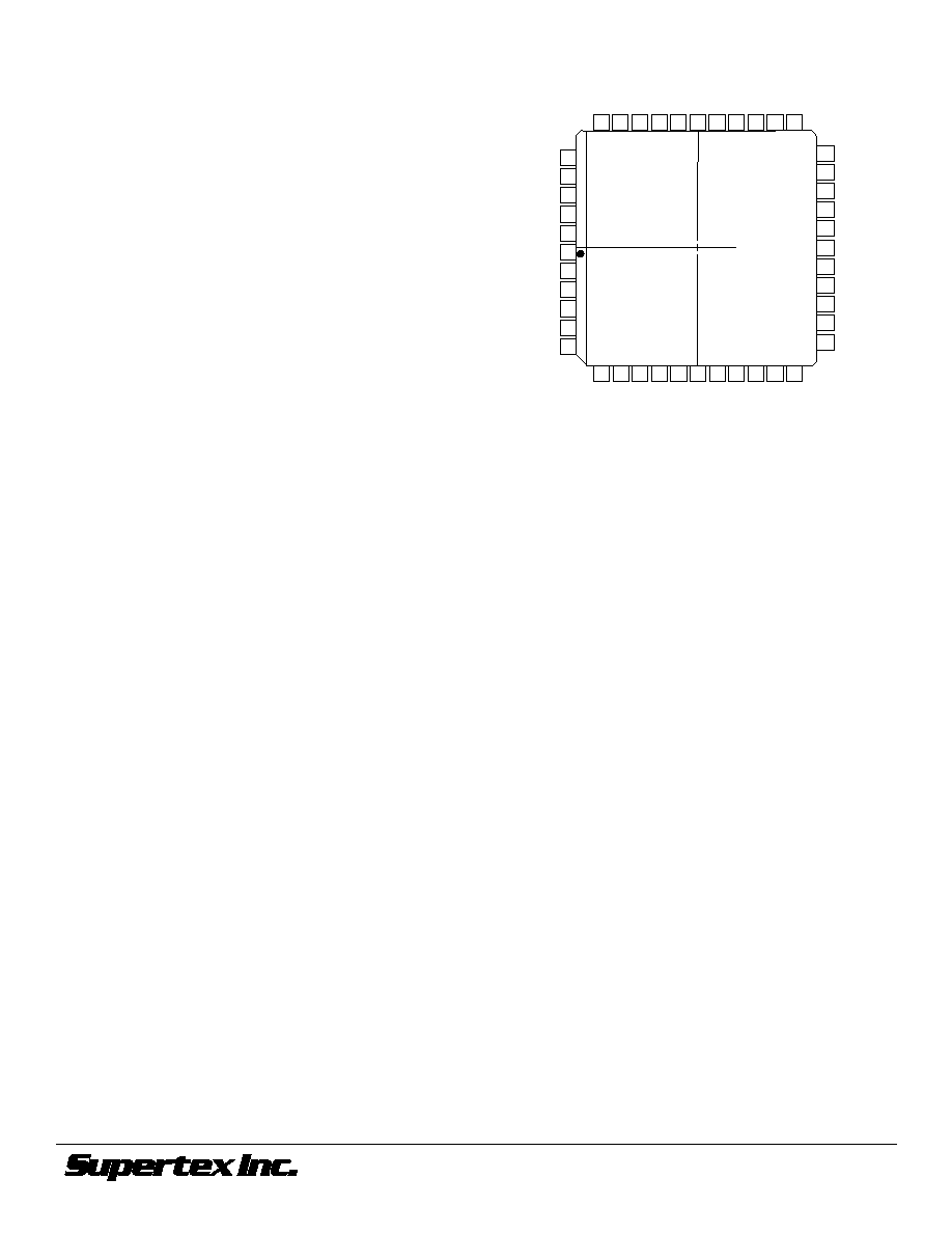
Pin Configuration
Package Outline
HV93
44 Pin J-Lead Package
Pin
Function
Pin
Function
1
HV
OUT
17
23
GND
2
HV
OUT
16
24
V
PP
3
HV
OUT
15
25
V
DD
4
HV
OUT
14
26
Latch Enable
5
HV
OUT
13
27
Data In
6
HV
OUT
12
28
Output Enable
7
HV
OUT
11
29
N/C
8
HV
OUT
10
30
HV
OUT
32
9
HV
OUT
9
31
HV
OUT
31
10
HV
OUT
8
32
HV
OUT
30
11
HV
OUT
7
33
HV
OUT
29
12
HV
OUT
6
34
HV
OUT
28
13
HV
OUT
5
35
HV
OUT
27
14
HV
OUT
4
36
HV
OUT
26
15
HV
OUT
3
37
HV
OUT
25
16
HV
OUT
2
38
HV
OUT
24
17
HV
OUT
1
39
HV
OUT
23
18
Data Out
40
HV
OUT
22
19
N/C
41
HV
OUT
21
20
N/C
42
HV
OUT
20
21
N/C
43
HV
OUT
19
22
Clock
44
HV
OUT
18
HV94
44 Pin J-Lead Package
Pin
Function
Pin
Function
1
HV
OUT
16
23
GND
2
HV
OUT
17
24
V
PP
3
HV
OUT
18
25
V
DD
4
HV
OUT
19
26
Latch Enable
5
HV
OUT
20
27
Data In
6
HV
OUT
21
28
Output Enable
7
HV
OUT
22
29
N/C
8
HV
OUT
23
30
HV
OUT
1
9
HV
OUT
24
31
HV
OUT
2
10
HV
OUT
25
32
HV
OUT
3
11
HV
OUT
26
33
HV
OUT
4
12
HV
OUT
27
34
HV
OUT
5
13
HV
OUT
28
35
HV
OUT
6
14
HV
OUT
29
36
HV
OUT
7
15
HV
OUT
30
37
HV
OUT
8
16
HV
OUT
31
38
HV
OUT
9
17
HV
OUT
32
39
HV
OUT
10
18
Data Out
40
HV
OUT
11
19
N/C
41
HV
OUT
12
20
N/C
42
HV
OUT
13
21
N/C
43
HV
OUT
14
22
Clock
44
HV
OUT
15
6
40
41
42
43
44
1
2
3
4
5
39 38 37 36 35 34 33 32 31 30 29
18
28
27
26
25
24
23
22
21
20
19
7
8
9
10 11 12 13 14 15 16 17
top view
44-pin J-Lead Package