1 4/15/2002-R.L2
Supertex, Inc. 1235 Bordeaux Drive, Sunnyvale, CA 94089 TEL: (408) 744-0100 FAX: (408) 222-4895 www.supertex.com
HV9606
Initial Release
HV9606 Current-Mode PWM Controller with Supervisor
Features
Synchronous Forward, Forward, and Flyback Controller
Lowest External Parts Count, Smallest Magnetics
Eliminates Bootstrap Transformer Winding
Supervisor Circuit Reduces Output Capacitance* up to 40%
Supervisor Circuit Functions as
�
P Supply Monitor and POR
15V to 250V Start-Up Regulator with START/STOP Control
<1mA Operating, <6
�
A Standby Input Current
V
DD
Powered Operation down to 2.9V
Charge Pump Gate Drive Supply
Programmable Soft Start
Under Voltage Lockout with Programmable Hysteresis
<50% Duty Cycle Operation
15kHz to 400kHz Fixed Frequency PWM Operation
Fault Tolerant Peer-to-Peer Synchronization
Precision
!
1% Band Gap Voltage Reference
Current Sense Leading Edge Blanking
Small SSOP-20 Footprint
*For short duration line loss, supervisor disables soft start if output
within tolerance when V
IN
returns and thus reduces holdup
requirements.
Applications
Powered Ethernet and VoIP Terminals
Cable Modems and Amplifiers
ISDN Network Terminations, Terminals and Adapters
Network Equipment
Servers, PCs and Peripheral Equipment
Telecommunication Systems and Terminals
Distributed Board Mounted Power
Battery Backup Systems
Portable Power Applications
Automotive and Heavy Equipment
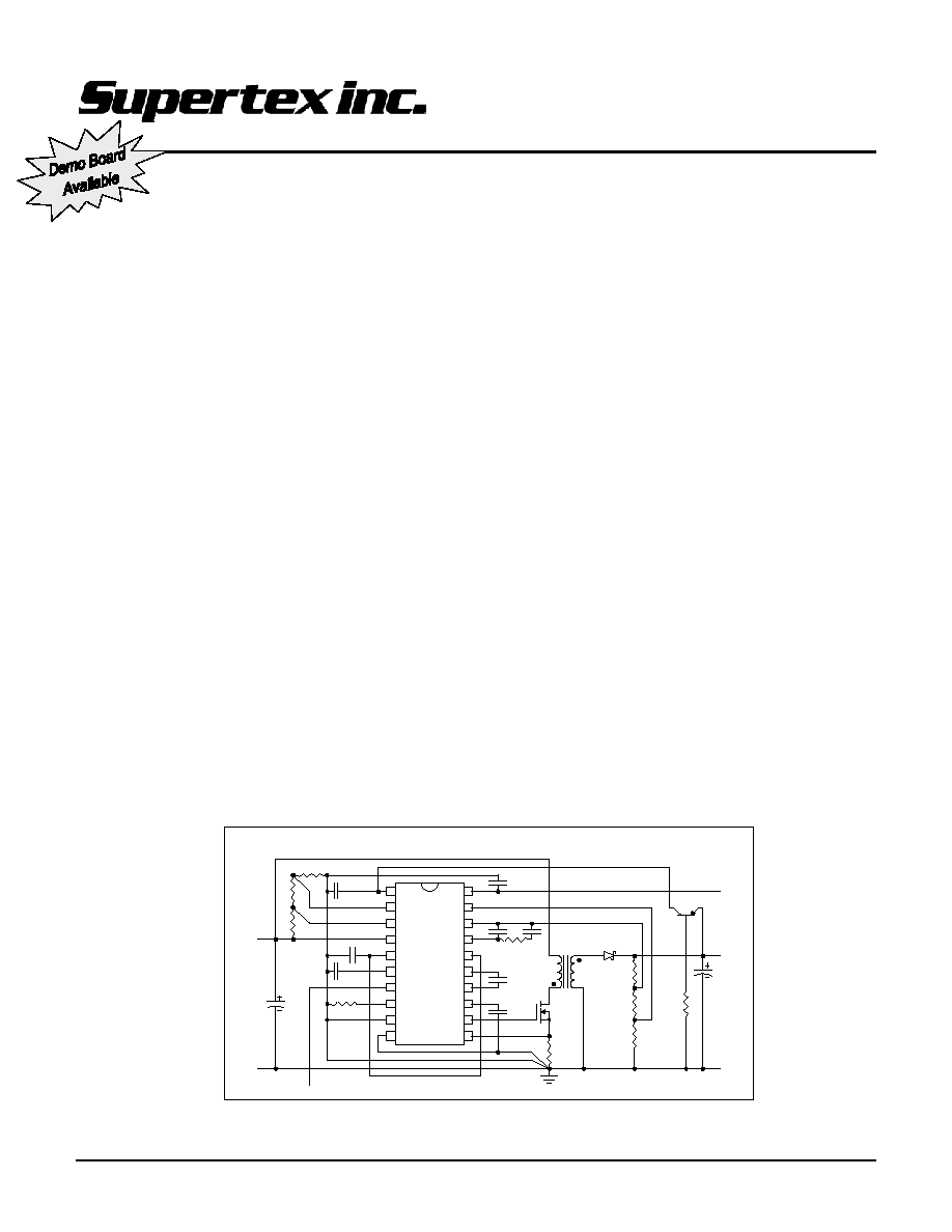
Typical Application Circuit
General Description
The HV9606 PWM controller allows the design of high efficiency
(>90%) power supplies for distributed board mounted power (BMP)
applications. Due to its high frequency capability it can provide
high currents (20A @ 3.3V) with small transformers and due to its
low internal operating voltage and current is also able to achieve
high efficiencies in low power applications.
The HV9606 utilizes fixed frequency current mode control with duty
cycle internally limited to <50%. It supports both isolated and non-
isolated topologies and provides all the necessary functions to
implement a flyback, forward or synchronous forward converter
with a minimum of external parts. Due to its low V
DD
operation the
bootstrap magnetic winding is eliminated in non-isolated
topologies. An on chip charge pump generates the gate drive
voltage for driving an external N-channel MOSFET and eliminates
the need for clamping by offering 250V immunity to high voltage
transients common in telecom and network systems. It conforms
to the requirements of IEEE 802.3 Powered Ethernet and ETR-080
ISDN specifications.
The oscillator is programmable and provides fault tolerant peer-to-
peer synchronization to other similar circuits or master clock. The
chip draws almost no current (<6
�
A @ V
IN
< 20V) until the
programmable START/STOP thresholds of the start-up regulator
are satisfied. It can also be powered via the V
DD
pin, rather than
the V
IN
pin, in the range of 2.9V to 5.5V.
Other functions include leading edge current sense blanking,
programmable SOFT START, precision
!
1% band gap reference
and a SUPERVISOR CIRCUIT. The SUPERVISOR can provide
housekeeping functions such as
�
P supply monitoring and reset,
soft start inhibit for rapid restart on short duration input voltage
interruption. It also minimizes input and output capacitance
requirements.
1
2
3
4
5
6
7
8
9
10
20
19
18
17
16
15
14
13
12
11
VDD
START
STOP
Vin
REF
SS
SYNC
RT
SGND
PGND
STATUS
SENSE
FB
COMP
NI
CA
CB
VX2
GATE
CS
H
V
9
6
0
6
To SYNC pin of other HV9606 PWMs.
+48V
GND
+3.3V
GND
To uP
RESET
Pin.
R1
R2
R3
R4
C1
C2
C3
C4
C6
C5
C7
C8
C9
C10
R5
R6
R7
R8
R9
M1
T1
D1
Q1
R10
10W Non-Isolated 48V to 3.3V Flyback Converter
2 4/15/2002-R.L2
HV9606
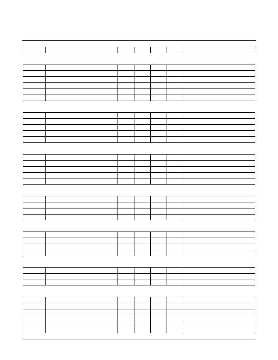
Electrical Characteristics
(-40
�
C
T
A
+85
�
C unless otherwise noted)
Symbol Parameter Min
Typ
Max
Units Conditions
Pre-Regulator/Start-up
V
IN
Regulator input voltage
15
250
V
I
IN
Input leakage current
6
�
A V
IN
20V, Start = 0V, Stop = 0V
I
IN
Input leakage current
50
�
A
V
IN
= 250V
V
DD(REG)
Regulator output voltage
2.8
2.9
3.0
V
Vin < 120V
UVLO
VDD
V
DD
Under voltage lockout threshold
2.7
2.8
2.9
V
V
DD
rising
UVLO
VDD
V
DD
Under voltage lockout hysteresis
100
200
mV
Supply
(Test Condition: 0.1
�
F CA to CB and 0.1
�
F VX2 to PGND)
V
DD
Operating
range
2.9 5.5 V
I
DD
Supply current
1.0
1.5
mA
GATE open, f
OSC
= 50 kHz, V
DD
= 3.3V
V
VX2
Gate drive charge pump supply
1.8xV
DD
V
UVLO
VX2
VX2 Under voltage lockout threshold
4.5
V
UVLO
VX2
VX2 Under voltage lockout hysteresis
0.4
V
Start/Stop Control
V
START
Start
threshold
6.44
7.00
7.56 V
V
IN
rising
V
STOP(MAX)
Maximum
voltage
13
V
V
STOP
Stop
threshold
6.44
7.00
7.56
V
V
IN
falling, V
START
= 0V
I
START
Start input current
50
nA
6.44V
V
START
7.56V, V
STOP
is open
I
STOP
Stop input current
50
nA
6.44
V
STOP
7.56V, V
START
to 10V via 10k
MOSFET Driver Output
(Test condition: V
VX2
= 5V)
V
GATE(HIGH)
Output high voltage
V
VX2
-0.2
V
I
GATE
= 10mA
V
GATE(LOW)
Output low voltage
0.15
V
I
GATE
= -10mA
t
R
Rise
time
30
50
nSec
C
LOAD
= 250pF
t
F
Fall
time
30
50
nSec
C
LOAD
= 250pF
Oscillator
f
OSC
Initial
accuracy
10 %
f
OSCRANGE
Oscillator Frequency Range
30
800
kHz
T
C
Temperature
coefficient
100
300
PPM/�C
f
OSC
= 100 kHz
f/f
Voltage stability
1
2
%
f
OSC
= 100 kHz, 2.9V V
DD
5.5V
SYNC
I
OSYNC
Sync output current
10
20
�
A
I
ISYNC
Sync input current
10
mA
V
SYNC
< 0.1 Volt
I
VSYNC
Sync input voltage absolute limits
-0.5
V
DD
+0.5
V
PWM
F
PWM
PWM Oscillation Frequency
15
400
kHz
F
PWM
= f
OSC
/2, Stability as f
OSC
above
D
MAX
Maximum duty cycle
49.99
%
f
OSC
= 30kHz
D
MAX
Maximum duty cycle
49
%
f
OSC
= 800kHz
D
MIN
Minimum pulse width before pulse drop out
130
195
nSec V
DD
= 3.3V
D
MIN
Minimum duty cycle
0
%
V
FB
> V
NI
, V
SS
> 2V
D
MIN
Minimum duty cycle
0
%
V
FB
< V
NI
, V
SS
< 0.1V
Supertex, Inc. 1235 Bordeaux Drive, Sunnyvale, CA 94089 TEL: (408) 744-0100 FAX: (408) 222-4895 www.supertex.com
3 4/15/2002-R.L2
HV9606
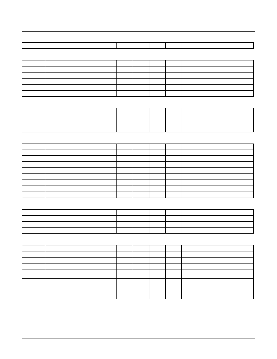
Electrical Characteristics � Continued
Symbol Parameter Min
Typ
Max
Units
Test
Conditions
Reference
V
REF
Reference output voltage
1.2402
V
T
A
= 25�C, 2.4V V
DD
5.5V
V
REF
Reference output voltage tolerance
1
%
T
A
= 25�C, 2.4V V
DD
5.5V
V
REF
Reference output voltage tolerance
2
%
-40�C
T
A
85�C, 2.4V V
DD
5.5V
V
REF
Load regulation
2
5
mV
0 < I
REF
< 0.1 mA
V
REF
Line
regulation
2 5
mV
2.4V
V
DD
5.5V
I
REF(SHORT)
Short circuit current
3
mA
V
REF
= GND
Current Sensing
(Test conditions: V
DD
= 3.3V)
V
CS
Usable control current sense range
0
0.59
V
V
CS
Current limit threshold
0.48V
REF
0.50V
REF
0.52V
REF
V
V
CS
Leading edge current sense blanking
time
85
nSec
t
DELAY
Current limit delay to output
70
120
nSec V
CS
= 0 to 1V step after blanking time
Error Amplifier
(Test conditions: 2.9V V
DD
5.5V)
I
FB
or I
NI
Input bias current
25
200
nA
V
FB
= 1.5V, V
NI
= 1.5V
V
FB
- V
NI
Input offset voltage
�3
mV
V
FB
= V
COMP
, V
NI
= 1.5V
V
CM
Common mode input range
0
V
DD
�0.1
V
A
VOL
Open loop voltage gain
65
dB
BW
Unity gain bandwidth
1
MHz
I
SOURCE
Output current sourcing
1
2
mA
V
FB
< V
NI
I
SINK
Output current sinking
-100
�
A
V
FB
> V
NI
V
COMP
Output voltage range
0
V
DD
�0.7
V
PSRR
Power supply rejection
50
dB
F
OSC
= 100 kHz
Soft Start
V
SS(LOW)
Soft start low output
0.1
V
V
DD
= 2.9V, V
SENSE
= 0V, V
CS
= 2.9V
V
SS(HI)
Soft start high output
2.5
V
DD
V
V
DD
= 2.9V, V
SENSE
= 2.9V, V
CS
= 2.9V
I
SS(HI)
Soft start output current
10
20
�
A
V
DD
= 2.9V, V
SENSE
= 2.9V, V
CS
= 2.9V
t
F
Soft start output fall time
10
�
Sec C
SS
= 0.1
�
F
Status Output
(Test conditions: 2.7V V
DD
5.5V)
I
SINK
Output current sinking
5
10
mA
V
STATUS
= 0.5V
I
SOURCE
Output current sourcing
10
20
�
A
V
STATUS
= (V
DD
- 0.5V)
V
STATUS(HIGH)
High output voltage
V
DD
-0.1 V
DD
V
No
load
V
STATUS(LOW)
Low output voltage
0.1
0.2
V
Sinking 2mA
V
SENSE(THLH)
Sense input threshold for rising input
0.85V
REF
+ 0.050
0.85V
REF
+ 0.075
0.85V
REF
+ 0.100
V V
STATUS
= LOW to HIGH transition
V
SENSE(THHL)
Sense input threshold for falling input
0.85V
REF
- 0.050
0.85V
REF
- 0.075
0.85V
REF
- 0.100
V V
STATUS
= HIGH to LOW transition
V
SENSE(HYST)
Sense input hysteresis
100
150
200
mV
Supertex, Inc. 1235 Bordeaux Drive, Sunnyvale, CA 94089 TEL: (408) 744-0100 FAX: (408) 222-4895 www.supertex.com
4 4/15/2002-R.L2
HV9606
Absolute Maximum Ratings*
V Input Voltage
-0.3V to +250V
Supply Voltage, V
DD
-0.3V to +6V
Gate Drive Supply Voltage, VX2
-0.3 to +15V
Operating Ambient Temperature Range -40
�
C to +85
�
C
Storage Temperature Range
-65
�
C to +150
�
C
Power Dissipation @ 25
�
C, SSOP
750mW
Power Dissipation @ 25
�
C, Plastic DIP 750mW
*All voltages referenced to SGND and PGND pins.
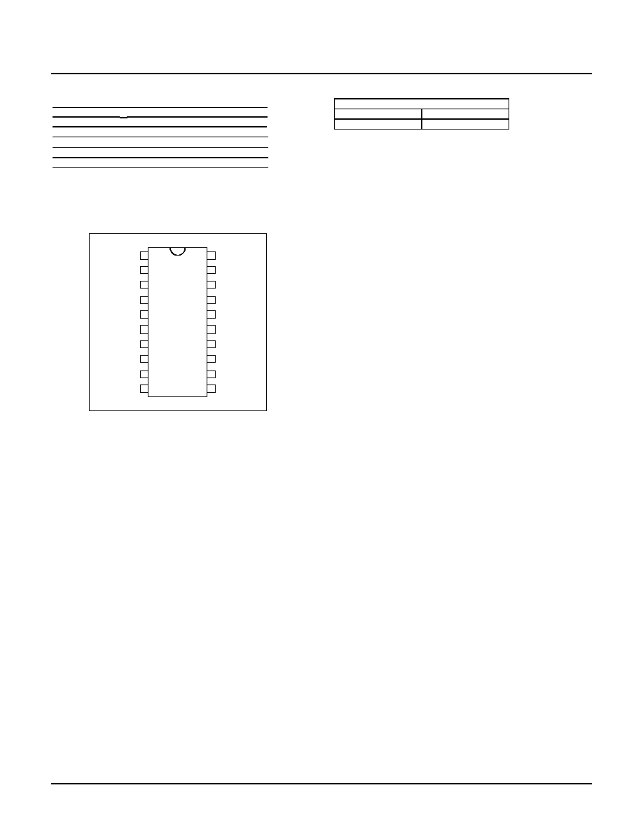
Ordering Information
Package Options
20-Pin SSOP
Dice
HV9606SP HV9606X
__________________________________________________________________________________________________________________
Pinout
1
2
3
4
5
6
7
8
9
10
20
19
18
17
16
15
14
13
12
11
H
V
9
6
0
6
VDD
START
STOP
Vin
REF
SS
SYNC
RT
SGND
PGND
STATUS
SENSE
FB
COMP
NI
CA
CB
VX2
GATE
CS
Pin Description
V
DD
� This is the supply pin for the PWM Logic and Analog circuits.
When the input voltage to the V
IN
pin exceeds the start voltage the
input regulator seeks to regulate the voltage on the capacitor
connected to this pin to a nominal 2.9V. After the PWM has
started, the bootstrap supply will regulate this voltage to a nominal
3.3V or 5V. With V
IN
connected to PGND the circuit can be
powered via this pin in the voltage range of 2.9V to 5.5V with a
nominal 2.8V UVLO.
START � The resistive divider from V
IN
sets the start-up regulator
start voltage.
STOP � The resistive divider from V
IN
sets the start-up regulator
stop voltage. A low power sleep mode function may be
implemented by pulling this pin to SGND.
V
IN
� This is the startup linear regulator input. It can accept DC
input voltages in the range of 15V to 250V. With START and
STOP programmed to more than 20V, the leakage current on this
pin is less than 6
�
A at V
IN
= 20V.
VREF � This pin provides a
!
1% tolerance reference voltage.
SS � A capacitor connected to this pin determines the soft start
time. Soft start may be initiated by a low VX2 voltage or an over
current condition when supervisor circuit STATUS output is low.
During short duration input interruptions when the output voltage
does not decay below programmed limits, the supervisor circuit
inhibits soft start to permit rapid recovery of the system.
SYNC � This I/O pin may be connected to the SYNC pin of other
HV9606 circuits and will cause the oscillators to lock to the highest
frequency oscillator. Synchronization to a master clock is possible
by means of an open collector or open drain logic gate or
optocoupler, provided the low duty cycle does not exceed 50%. If
synchronization is utilized then a pull up resistor to V
DD
is required
to overcome the effects of parasitic capacitance on the circuit
board. The value of the resistor required will depend on the
operating frequency and master clock duty cycle.
RT � The resistor connected from this pin to SGND sets the
frequency of the internal oscillator by setting the charging current
for the internal timing capacitor. The PWM output frequency is one
half the oscillator frequency.
SGND � Common connection for all Logic and Analog circuits.
PGND � Common connection for Gate Driver circuit.
CS � This is the current sense input. Under normal operation the
over current limit is triggered when the voltage on this pin exceeds
0.5V
REF
, however, current sensing is blanked during the first 85ns
on time of the MOSFET to prevent false triggering during the turn
on switching transition. The loop control operating peak current
sense may be set to any level below 0.5V
REF
.
GATE � This push-pull CMOS output is designed to drive the gate
of an N-Channel power MOSFET.
VX2 � This is the supply pin for the Gate Driver circuit and is
generated by the Charge Pump V
DD
voltage doubler circuit. It
should be bypassed to PGND with a capacitor, typically 0.1
�
F.
CA and CB � The charge pump circuit uses a capacitor (typically
0.01
�
F) connected between these pins to generate the VX2
voltage.
NI � High impedance non-inverting input of the error amplifier.
COMP � The output of the error amplifier.
FB � High impedance inverting input of the error amplifier.
SENSE � This is the input pin to the supervisory circuit. On a
rising input voltage the circuit changes state at a nominal 0.85V
REF
+ 0.075V. When the input voltage is decaying the circuit changes
state a nominal 0.85V
REF
� 0.075V.
STATUS � This is the output of the supervisory circuit. When the
sense-input voltage is high, this output is pulled up to V
DD
by a
10
�
A current source and the Soft Start function is disabled. When
the sense-input is low, this output is pulled low and it may be used
to directly control the reset of a microprocessor or it may be used
to drive an optocoupler or LED indicator.
Supertex, Inc. 1235 Bordeaux Drive, Sunnyvale, CA 94089 TEL: (408) 744-0100 FAX: (408) 222-4895 www.supertex.com
5 4/15/2002-R.L2
HV9606
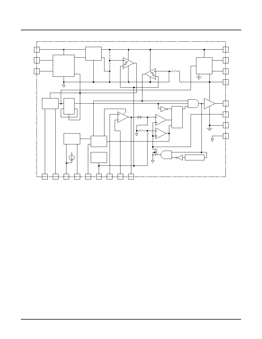
Functional Block Diagram
C
Vdd
UVLO
C
Start-Up
Regulator
Vdd
Vin
STOP
START
Regulator
Enable
RT
SYNC
Bandgap
Reference
Generator
Programable
Start/Stop
Circuit
FB
A
COMP
C
S
R
R
Q
CS
Supervisor
Circuit
Soft
Start
Circuit
Oscillator
SS
STATUS SENSE
GATE
Soft
Start
Enable
VREF
PGND
CLK
D
Q
Q
_
CLR
___
85 nS Delay
Voltage
Doubler
VX2
CA
CB
SGND
C
VX2
UVLO
Vdd
NI
R
R
Current
Limit
Oscillator
Enable
Functional Description
The HV9606 is composed of several functional blocks. The
operation of each of these blocks is described in the following
sections.
Programmable Start/Stop Control Circuit
(Programmable Under Voltage Lockout and Hysteresis)
The START/STOP control circuit is a novel version of a
programmable under voltage lockout with programmable
hysteresis circuit. It is novel, because it requires zero power (other
than the current in the resistor divider) and keeps the startup
regulator shut down until the START threshold voltage is
exceeded, allowing the HV9606 to achieve its low input leakage
current of <6
�
A.
One can think of the circuit as a transparent latch, such that its
output is high when the START pin is above its threshold voltage
and is latched when the STOP pin is at a voltage greater than the
START pin voltage. It is unlatched when the STOP pin voltage
falls below its threshold voltage and the START pin is below its
threshold voltage.
These operating conditions are met by using a voltage divider
consisting of three resistors (see typical application circuit). The
voltage drop on the resistor connected to ground controls the
START voltage and the additional voltage drop on the middle
resistor sets the hysteresis and controls the STOP voltage. Setting
the value of the middle resistor to zero results in zero hysteresis.
Provided the START and STOP pin input currents are negligible in
comparison to the chosen resistor divider current, the resistor
values may be calculated using the following equations:
R3 = (V
START
/ V
IN-Start
) x (V
IN-Stop
/ I
Resistor
)
R2 = [(V
STOP
/ V
IN-Stop
) x (V
IN-Stop
/ I
Resistor
)] � R3
R1 = (V
IN-Operating
/ I
Resistor
) - R2 - R3
Where:
V
START
is the START pin threshold voltage (nominal 7V)
V
STOP
is the STOP pin threshold voltage (nominal 7V)
V
IN-Start
is the input voltage at which starting is desired
V
IN-Stop
is the input voltage at which shutdown is desired
I
Resistor
is the resistor divider current (>1
�
A)
Supertex, Inc. 1235 Bordeaux Drive, Sunnyvale, CA 94089 TEL: (408) 744-0100 FAX: (408) 222-4895 www.supertex.com

6 4/15/2002-R.L2
HV9606
Functional Description � Continued
Start-Up Regulator
The start-up regulator guarantees a maximum V
IN
pin leakage
current of 6
�
A at 20V at the V
IN
pin while it is inhibited by the
START/STOP circuit. When the effective input voltage exceeds
the programmed START voltage, the regulator is turned on and
seeks to provide a nominal 2.9V at the V
DD
pin, which is the supply
voltage for all internal circuitry within the HV9606 except the
start/stop circuit. This regulator is capable of input voltages up to
250 Volts, which is the typical maximum arrester voltage limit used
to provide protection on telephone wires. Due to the high voltage
rating of the regulator the HV9606 can be used for applications
operating from rectified AC mains up to 140Vrms. The regulator
can supply a minimum of 5mA, which is sufficient to power the
internal circuitry and provide gate drive power for the external
MOSFET until the bootstrap circuit from the output of the PWM
drives the voltage on the V
DD
pin higher than the regulator set
point. This forces the regulator to turn off and reduce the input
current at the Vin pin to leakage levels. The V
DD
pin is typically
bypassed with a capacitor of at least 1
�
F, which provides the peak
currents required by the voltage doubler and in turn the gate driver
for the external MOSFET.
For low power applications the circuit may be operated without
bootstrapping. Care should be taken to assure that the power
dissipation in the regulator does not become excessive, as it might
be if the input voltage is high and the gate drive energy required is
high (operating at high frequency).
Low voltage operation of the HV9606 is also possible by powering
V
DD
from supply voltages of 2.9V to 5.5V. In these applications the
Vin, START and STOP pins should be connected to SGND pin.
When powering only via V
DD
, the START/STOP control is not
available and the startup regulator circuit is not used.
V
DD
Under Voltage Lockout
To guarantee correct operation, internal circuitry is held reset by an
under voltage lockout (V
DD
UVLO) until the regulator output voltage
is at least 100mV below the startup regulator set point. To
guarantee stable starting the V
DD
UVLO has a hysteresis of
100mV.
Oscillator
The oscillator circuit operates at twice the PWM output frequency.
The frequency can be programmed in the range of 30kHz to
800kHz by means of a single resistor connected from the RT pin to
SGND. For a given frequency the value of the resistor can be
calculated using the following equation:
R
T
= [(1 / f
OSC
) �1x10
-7
] / 42.6x10
-12
Synchronization
The SYNC pin is an input/output (I/O) port to a unique fault tolerant
peer-to-peer and/or to master clock synchronization circuit. For
synchronization the SYNC pins of multiple HV9606 based
converters can be connected together and may also be connected
to the open drain/collector output of an external master clock.
When connected in this manner the oscillators will lock to the
device with the highest operating frequency. The LOW duty cycle
of an external master clock should not exceed 50%. When
synchronized in this manner, a permanent logic HIGH or LOW
condition on the SYNC pin will result in a loss of synchronization,
but the HV9606 based converters will continue to operate at their
individually set operating frequency. For this reason the SYNC pin
is considered fault tolerant, since loss of synchronization will not
result in total system failure.
Depending on the cumulative parasitic capacitance on the SYNC
pin when connected in the above manner a pull up resistor may be
required from the SYNC pin to the V
DD
pin on each HV9606 based
DC/DC converter circuit. The value of the resistor will depend on
the cumulative parasitic capacitance and operating frequency.
Voltage Doubler
The HV9606 can operate on internal voltages ranging from 2.9V to
5.5V. It may be difficult to find power MOSFETs capable of
operating with such low gate drive voltages. For this reason the
HV9606 incorporates a voltage doubler circuit that generates a
voltage on the VX2 pin that is approximately two times the V
DD
voltage. This circuit uses capacitive charge transfer methods and
requires the connection of a capacitor (typically 0.01
�
F) between
the CA and CB pins as well as an energy storage capacitor
(typically 0.1
�
F) connected from the VX2 pin to PGND pin. The
voltage doubler operates at the PWM output frequency.
The gate driver output on the GATE pin operates from the VX2
voltage, logic level (5Volt) gate power MOSFETs may be used
when V
DD
is bootstrapped at 3.3V or standard (10V) gate
MOSFETs may be used when V
DD
is bootstrapped at 5V.
VX2 Under Voltage Lockout
To guarantee that sufficient gate drive voltage is available, an
under voltage lockout circuit (VX2 UVLO) monitors the VX2
voltage. If the VX2 voltage drops below 4.5V the gate driver output
of the PWM circuit is inhibited to prevent damage to the power
MOSFET. This under voltage lockout has a hysteresis of 400mV
to prevent spurious operation.
Band Gap Reference
The operating limits of all internal circuits, except the
START/STOP circuit, are based on the
!
1% tolerance band gap
reference voltage available on the REF pin. It is capable of
delivering 100
�
A for use by external circuitry without degrading the
reference. A bypass capacitor of at least 0.1
�
F should be
connected from the REF pin to SGND pin.
Supertex, Inc. 1235 Bordeaux Drive, Sunnyvale, CA 94089 TEL: (408) 744-0100 FAX: (408) 222-4895 www.supertex.com

7 4/15/2002-R.L2
HV9606
Functional Description � Continued
Current Sense and Current Limit
Current sensing is accomplished by means of a resistor connected
in series with the source of the external power MOSFET. There
are two independent comparators monitoring the voltage drop
across this resistor. One provides absolute peak current limiting at
0.5V
REF
and the other provides peak current feedback to the PWM
control loop.
Gate charge, capacitive loading and reverse recovery of output
rectifier reflected to the drain of the power MOSFET results in high
current spike at the positive leading edge of gate drive when the
MOSFET is turning on. This can result in false tripping of the
current limit comparator or incorrect operation of the control loop.
To prevent this condition an 85nSec leading edge current sense
blanking circuit is incorporated in the HV9606. This blanking
period is sufficient in most applications to achieve stable operation.
However, additional filtering of the MOSFET turn on current spike
may be added by connecting a resistor in series with the (CS)
current sense pin and a capacitor from the current sense pin to
SGND pin.
Error Amplifier
The error amplifier has a minimum gain bandwidth of 1MHz. The
inverting and non-inverting inputs are available respectively at FB
and NI pins and the amplifier output is available at the COMP pin.
Maximum application flexibility is provided to the designer by
having all terminals of the error amplifier available. The design of
the error amplifier prevents its output from saturating to the high
rail (V
DD
) thus providing very fast slew recovery capability.
Soft Start Control Circuit
The soft start circuit provides a nominal constant current output of
10
�
A at the SS pin for charging a capacitor connected to this pin.
The instantaneous voltage on the SS pin determines the high limit
of the error amplifier, thus forcing the PWM to start at minimum
output duty cycle and slowly increase the duty cycle until stable
closed loop operation is achieved. The value of the capacitor
should be selected to achieve this stable closed loop operation
before the voltage on the SS pin exceeds 1.2V at maximum output
load on the DC/DC converter.
Soft start can only be initiated if the STATUS output of the
SUPERVISOR circuit is low. The SS pin is pulled low, discharging
the capacitor and engaging soft restart whenever the VX2 UVLO
detects a low gate drive voltage.
PWM Circuit
The current mode PWM circuit operates at one half the oscillator
frequency with a duty cycle guaranteed not to exceed 50%. Its
minimum pulse width (typically 130nSec) provides a wide dynamic
control range especially when operating at low frequencies.
For the dynamic control range required by a given application the
maximum operating frequency can be determined using the
following equations.
t
ON
= ( V
IN(MAX)
/ V
IN(MIN)
) x ( P
OUT(MAX)
/ P
OUT(MIN)
) x D
MIN
f
OSC
= 2 f
PWM
< 1 / t
ON
Where t
ON
is the maximum gate drive output on time, V
IN(MAX)
and
V
IN(MIN)
are the maximum and minimum input voltage, P
OUT(MAX)
and
P
OUT(MIN)
are the maximum and minimum output power, D
MIN
is the
worst case minimum gate drive output duty cycle (195nSec), f
PWM
is the maximum gate drive switching frequency and f
OSC
is the
maximum oscillator frequency.
Supervisor Circuit
The designer may use this voltage monitor circuit for various
applications. The supervisor circuit controls the function of the soft
start circuit, which will be enabled when the STATUS output pin is
in a low state. The STATUS output pin is low when the voltage on
the SENSE pin is less than 0.85V
REF
� 100mV.
The supervisory circuit can be used to monitor the output voltage
of the DC/DC converter. When used in this manner the STATUS
output pin may be used as a supply monitor and power on reset
(POR) for a micro controller whenever the supply voltage decays
to a programmed voltage level. Using it in this manner in a non-
isolated topology, where the output voltage is used for
bootstrapping V
DD
, it will inhibit soft start as long as the output is
within programmed limits, thereby providing a rapid restart after a
short duration input voltage dropout. This allows the minimization
of both input and output capacitors for a given system hold up time
requirement. In an Isolated topology, sizing the V
DD
capacitor for a
hold up time greater than the output hold up time requirement will
similarly permit the minimization of the input and output capacitors.
The supervisory circuit can also be used as a high accuracy low
input voltage detection and inhibit circuit by connecting the
STATUS pin to the SS pin. Since the status pin has a 10
�
A
internal pull up it will double the charging current of the soft start
capacitor, thus the soft start capacitor value needs to be doubled
for the same soft start time. The SENSE pin may be connected
through a resistor divider to any monitored voltage source (other
than the output of the HV9606 based DC/DC converter) or to a
logic output. When the voltage on the SENSE pin falls below
0.85V
REF
� 100mV, the SS pin will be pulled low, thereby inhibiting
the gate drive output and shutting down the converter. The
oscillator will operate even though the GATE output is held low and
the SYNC I/O pin will maintain synchronization with other system
components or provide a clock signal to the system.
Shut Down / Inhibit Operation
The HV9606 may be shut down or inhibited depending on the
system requirements.
Pulling the STOP pin down to SGND will shut down the HV9606,
placing it in a zero power (leakage only) mode where even the
oscillator is halted. This pull down may be accomplished with a
discrete MOSFET, an optocoupler, or the open drain/collector
output of a logic gate with at least 20V breakdown rating. Using
this shut down method will cause the SYNC pin to be pulled low,
thus synchronization of other components connected to the SYNC
line will be lost.
Provided the input voltage remains above the programmed stop
threshold, inhibit of the PWM can be achieved by pulling the SS
pin low to SGND, thereby forcing the gate drive output to a
permanent low state and guaranteeing a soft restart when SS pin
pull down is released. The internal start up regulator will power the
HV9606 thus the oscillator will operate and the SYNC I/O pin will
maintain synchronization with other system components or provide
a clock signal to the system. This pull down could be
accomplished with a discrete MOSFET, an optocoupler, or the
open drain/collector output of a logic gate with at least a 5V
breakdown rating.
Supertex, Inc. 1235 Bordeaux Drive, Sunnyvale, CA 94089 TEL: (408) 744-0100 FAX: (408) 222-4895 www.supertex.com
8 4/15/2002-R.L2
HV9606
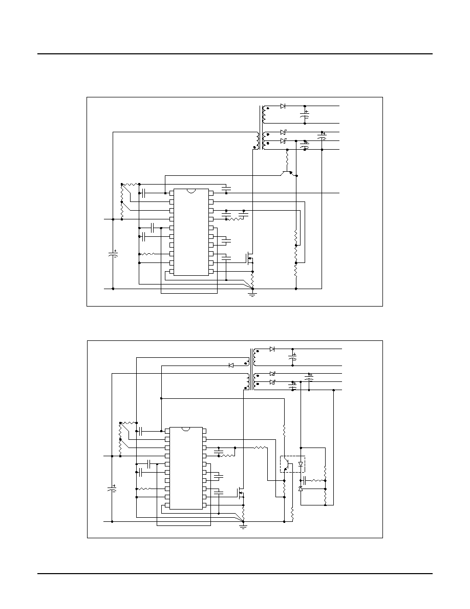
Application Information
Typical Semi-Isolated ISDN Circuit
1
2
3
4
5
6
7
8
9
10
20
19
18
17
16
15
14
13
12
11
VDD
START
STOP
Vin
REF
SS
SYNC
RT
SGND
PGND
STATUS
SENSE
FB
COMP
NI
CA
CB
VX2
GATE
CS
H
V
9
6
0
6
+48V
GND
+3.3V
GND
To uP RESET pin.
R1
R2
R3
R4
C1
C2
C3
C4
C6
C5
C7
C8
C9
C10
R5
R6
R7
R8
R9
M1
T1
D1
Q1
R10
C11
C12
+5V
D2
D3
+
-
Isolated 40V
1.5W Flyback Converter
Typical Isolated ISDN Circuit
1
2
3
4
5
6
7
8
9
10
20
19
18
17
16
15
14
13
12
11
VDD
START
STOP
Vin
REF
SS
SYNC
RT
SGND
PGND
STATUS
SENSE
FB
COMP
NI
CA
CB
VX2
GATE
CS
H
V
9
6
0
6
+48V
GND
+3.3V
COM
R1
R2
R3
R4
C1
C2
C3
C4
C6
C5
C7
C8
C9
R5
R6
R7
R8
M1
T1
D1
R10
C10
+5V
D2
D3
+
-
Isolated 40V
D4
R11
6N135
R12
R13
R14
TL431
1.5W Isolated Flyback Converter
C11
Supertex, Inc. 1235 Bordeaux Drive, Sunnyvale, CA 94089 TEL: (408) 744-0100 FAX: (408) 222-4895 www.supertex.com
9 4/15/2002-R.L2
HV9606
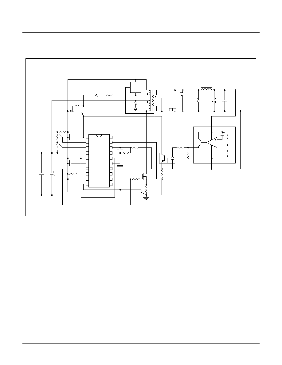
Application Information
Typical Board Mounted Power (BMP) Supply
1
2
3
4
5
6
7
8
9
10
20
19
18
17
16
15
14
13
12
11
VDD
START
STOP
Vin
REF
SS
SYNC
RT
SGND
PGND
STATUS
SENSE
FB
COMP
NI
CA
CB
VX2
GATE
CS
H
V
9
6
0
6
+48V
GND
+
-
R1
R2
R3
R4
C1
C3
C5
C4
C6
C7
C8
R8
R5
R6
R9
M1
T1
D1
D2
C2
R7
2 x Si4884DY
M2 and M3
M4 and M5
2 x Si4884DY
L1
IRF530S
B320A
1N4148
1.23V
(+) IN
(-) GND
OUT
31K
Rf
COMP
LM3411
Optional Connection to SYNC Pin
of other HV9606 DC/DC Converters
or Master Clock
C9
C10
C11
R10
48V to 3.3V @ 20A Isolated Synchronous Forward Converter with Resonant Core Reset
MOC207
U1
U3
U2
3.3V
@
20A
R13
D4
D5
R11
R12
D3
Q1
Active
Snubber
Circuit
Supertex, Inc. 1235 Bordeaux Drive, Sunnyvale, CA 94089 TEL: (408) 744-0100 FAX: (408) 222-4895 www.supertex.com