 | –≠–ª–µ–∫—Ç—Ä–æ–Ω–Ω—ã–π –∫–æ–º–ø–æ–Ω–µ–Ω—Ç: HV9608TS | –°–∫–∞—á–∞—Ç—å:  PDF PDF  ZIP ZIP |
Supertex, Inc.
∑
1235 Bordeaux Drive, Sunnyvale, CA 94089
∑
Tel: (408) 222-8888
∑
FAX: (408) 222-4895
∑
www.supertex.com
Active Clamp Current-Mode PWM Controller
Features
Peak current-mode PWM Controller
Two complementary MOSFET drivers
Programmable deadtime between drivers
High current gate drivers for main and auxiliary outputs
Internal high voltage (12V to 250V) start-up regulator
Programmable V
IN
undervoltage lockout and hysteresis
V
DD
supply operation from 7.8V to 12V
Fixed frequency PWM operation from 25KHz to 800KHz
>50% duty cycle operation (up to 95%)
Programmable slope compensation
Programmable max duty-cycle/volt-second clamp
Capacitor programmable soft-start
Cycle-by-cycle current limiting
100ns current sense leading edge blanking
2 MHz error amplifier
Applications
Networking
Telecommunication Systems and Terminals
IEEE 802.3af PoE PD Devices
SANS, Servers & Workstations
High Efficiency Instrumentation Supplies
High Efficiency Supplies for Portable Equipment
Description
The HV9608 provides a single chip, optimized peak current
mode control solution for design of high performance PWM
converters using the active-clamp transformer flux reset.
Due to its programmable slope compensation feature, the
HV9608 allows operation beyond 50% duty cycle. Zero-
voltage switching can be accomplished through using the
programmable deadtime timers. The switching frequency
can be programmed from 25kHz to 800kHz using a single
resistor. The internal high voltage startup circuit can ensure
start-up from the input voltage from 12V to 250V. It can also
maintain the HV9608 in operation when the external
"bootstrap" power supply is not available. The startup
regulator is disconnected as soon as the HV9608 becomes
powered from the bootstrap winding. The HV9608 offers a
programmable soft start feature using a single external
capacitor. The cycle by cycle current limit feature can
protect the converter from overheating and damage by
limiting the output over current. The HV9608 will maintain
the cycle-by-cycle current limiting mode for a period of time
programmed by the soft start capacitor value. The HV9608
includes a single pin UVLO circuit that allows independent
accurate setting of both the turn-on and the turn-off
threshold voltage. A programmable volt-second clamp
reduces voltage stress of the switching devices. The
HV9608 is available in a space-saving TSSOP-16 package.
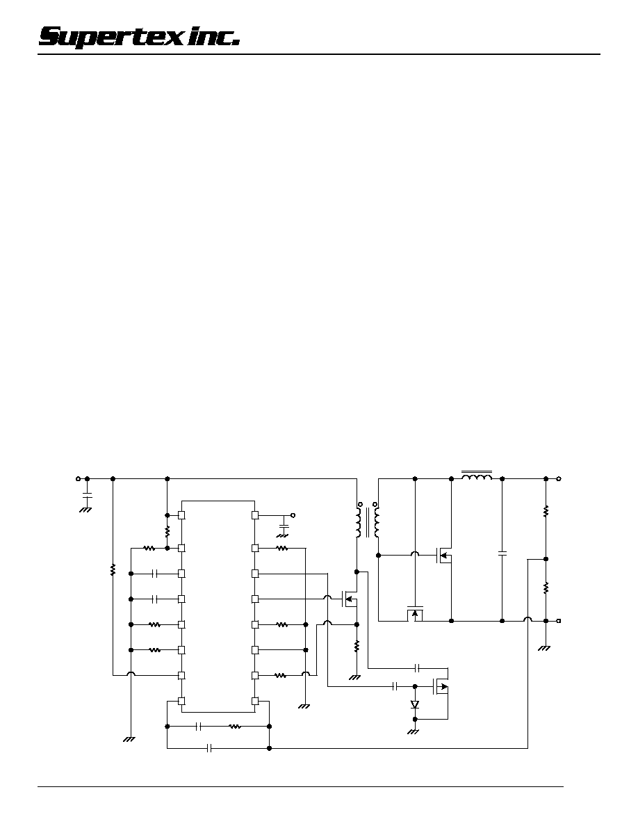
Typical Application Circuit
VIN
C
IN
VIN
HV9608
1
UVLO
2
R1
R2
3
4
5
6
7
8
C1
C
SS
R
SC1
R
T
R
VS
REF
SS
RT
SC
VS
COMP
16
15
14
13
12
11
10
9
VDD
AGATE
GATE
DT1
DT2
GND
CS
FB
C
Z
R
P
C
P
R
DT2
R
DT1
C
2
VDD
R
S
Q
1
C
4
C
3
Q
2
Q
3
Q
4
L
F
C
F
R
3
R
4
Vo
+
-
T
1
R
SC2
HV9608
Initial Release
A122104
HV9608
2
A122104
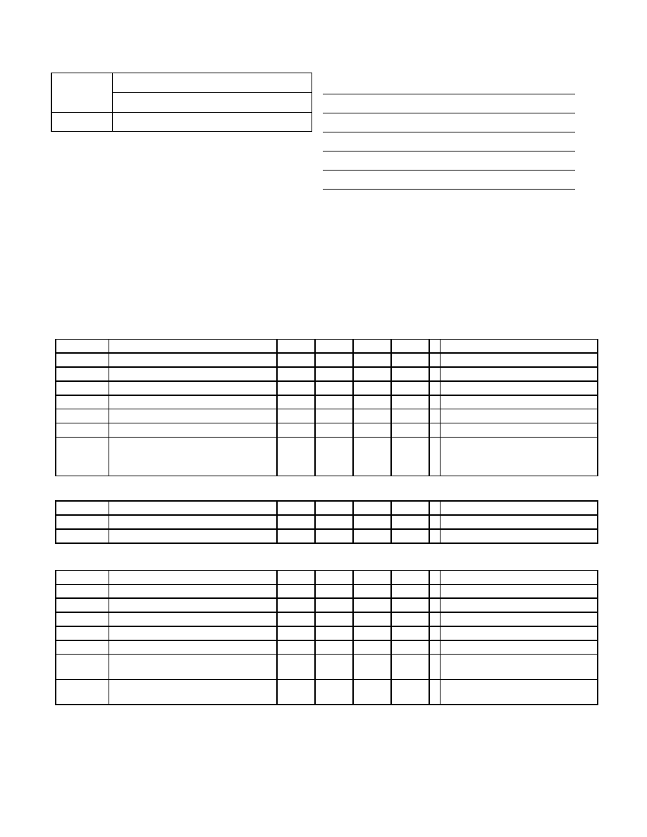
Electrical Characteristics
(The * denotes the specifications which apply over the full operating temperature
range of -40
∞
C < T
A
< +85
∞
C, otherwise the specifications are at T
A
= 25
∞
C, V
D D
= 10V, unless otherwise noted)
V
IN
_Pre-Regulator/Start-up/ V
DD
_Supply
Symbol Parameter Min
Typ.
Max
Units Conditions
V
IN
Regulator input voltage
12
250
V
I
IN,MAX
Maximum regulator current
20
mA V
IN
= 24V, V
DD
= 9.2V
V
DD,REG
Regulator output voltage
9.27
9.46
9.65
V
V
IN
[12V ≠ 250V]
V
DD, MAX
Supply voltage range
12
V
To guarantee table parameters
V
DD,STOP
V
DD
under voltage threshold
7.58
7.74
7.90
V
V
DD
falling
V
DD,START
V
DD
startup voltage
8.33
8.5
8.67
V
V
DD
rising
I
DD,OFF
Supply standby quiescent current 1.25
1.8
mA
R
T
= 110 K
; R
DT1
= 80K
;
R
DT1
= 80K
; UVLO tied to
ground;
Under Voltage Lockout (UVLO)
Symbol Parameter Min
Typ.
Max
Units Conditions
V
th,UVLO
UVLO threshold voltage
1.112 1.135 1.158
V
*
I
HYS,UVLO
UVLO hysteresis current
14
µ
A Guaranteed by design
GATE/AGATE_MOSFET Driver Output
Symbol Parameter Min
Typ
Max
Units Conditions
t
R1
Main gate rise time
40
60
nSec C
LOAD
= 1nF
t
F1
Main gate fall time
20
30
nSec C
LOAD
= 1nF
t
R2
Auxiliary gate rise time
40
60
nSec C
LOAD
= 0.5nF
t
F2
Auxiliary gate fall time
20
30
nSec C
LOAD
= 0.5nF
R
DT1
, R
DT2
Dead time control resistor range
40
400
K
d
1
Rising edge delay from AGATE to
GATE
80 105 130
nSec
R
DT1
= 80K
d
2
Falling edge delay from GATE to
AGATE
100 400
nSec
R
DT2
= 80K
Absolute Maximum Ratings*
Input Voltage, V
IN
-0.3V to +250V
Supply Voltage, V
DD
+13.5V
max
Operating Ambient Temperature Range
-40∞C to +85∞C
Operating Junction Temperature Range
-40∞C to +125∞C
Storage Temperature Range
-65∞ to +150∞C
Power Dissipation @ 25∞C, TSSOP
1000mW
Ordering Information
Package Options
DEVICE
16-Pin TSSOP
HV9608 HV9608TS
*All voltages referenced to GND pin.
Stresses beyond those listed under "Absolute Maximum Ratings" may cause
permanent damage to the device. These are stress ratings only, and
functional operation of the device at these or any other conditions beyond
those indicated in the operational sections of the specifications is not
implied. Exposure to absolute maximum rating conditions for extended
periods may affect device reliability.
HV9608
3
A122104
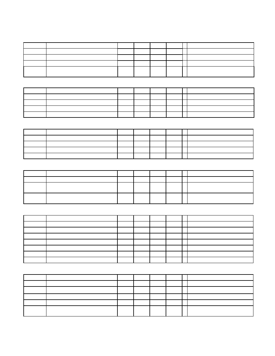
Electrical Characteristics
(continued from page 2) (The * denotes the specifications which apply over the full
operating temperature range of -40
∞
C < T
A
< +85
∞
C, otherwise the specifications are at T
A
= 25
∞
C, VDD = 10V, unless otherwise noted)
R
T
_Oscillator
Symbol Parameter Min
Typ
Max
Units Conditions
f
OSC,MIN
Minimum operating frequency
25
KHz R
T
= 1.862M
f
OSC,MAX
Maximum operating frequency
800
KHz R
T
= 52.3K
f
OSC
Frequency
variation
220
250
280
KHz
* R
T
= 169K
f/f
VDD supply voltage stability of
frequency
3
%
R
T
= 169K
, 7.8V < V
DD
< 12V
PWM
Symbol Parameter Min
Typ
Max
Units Conditions
D
MAX
Maximum GATE duty cycle
95
%
* f
OSC
= 100KHz (R
T
= 453K
)
D
MAX
Maximum GATE duty cycle
85
%
* f
OSC
= 800KHz (R
T
= 52.3K
)
D
MIN
Minimum GATE duty cycle
0
%
D
MIN
Minimum GATE duty cycle
0
%
Reference
Symbol Parameter Min
Typ
Max
Units
Conditions
V
REF
Reference output voltage
1.112 1.135 1.158
V
*
I
SRC
Maximum sourcing current
2
mA
V
REF
Load regulation
5
mV 0 < I
REF
< 2 mA
V
REF
Line regulation
20
mV 7.8V < V
DD
< 12V
Current Sensing
Symbol Parameter Min
Typ
Max
Units
Conditions
V
CS
Current limit threshold voltage
0.58
0.6
0.62
V
t
BLANK
Leading edge current sense
blanking time
100 nSec
t
DELAY
Current limit delay to output
70
120
nSec
V
CS
= 0 to 1V step after blanking
time
Error Amplifier
Symbol Parameter Min
Typ
Max
Units
Conditions
I
FB
Input
bias
current
25
200
nA
V
FB
= V
COMP
V
FB
FB input voltage
1.112 1.135 1.158
V
V
FB
= V
COMP
A
VOL
Open loop voltage gain
70
dB
BW
Unity gain bandwidth
2
MHz
I
SOURCE
Maximum output current sourcing
2
mA
I
SINK
Maximum output current sinking
4
mA
V
COMP
Output clamped voltage
3.3
3.45
3.6
V
Soft Start
Symbol Parameter Min
Typ
Max
Units
Conditions
V
SS,LOW
Soft start low output
0.1
V
V
SS,HI
Soft start high output
5.25
5.45
5.65
V
I
SS,HI
Soft start output current
7
µ
A
t
F
Soft start output fall time
10
µ
Sec C
SS
= 0.1
µ
F; V
FB
= V
COMP
;
I
SS,LO
Pulse-by-pulse current limit mode
sink current
7
µ
A
HV9608
4
A122104
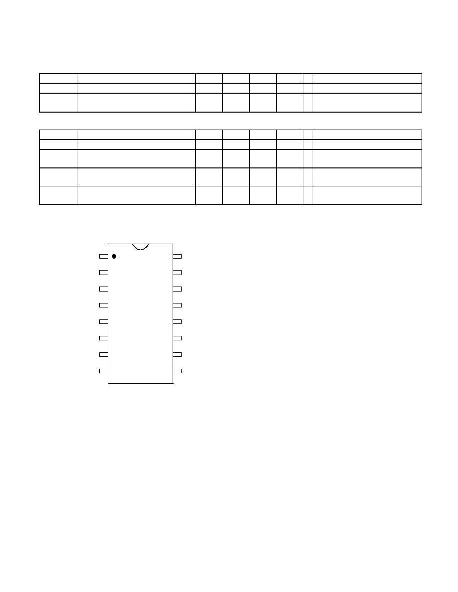
Electrical Characteristics
(continued from page 3)
(The * denotes the specifications which apply over the full
operating temperature range of -40
∞
C < T
A
< +85
∞
C, otherwise the specifications are at T
A
= 25
∞
C, V
DD
= 10V, unless otherwise noted)
Slope Compensation
Symbol Parameter Min
Typ
Max
Units
Conditions
R
SC
Slope compensation resistor range
5
k
I
RAMP,PEAK
Slope compensation ramp peak
current
125 150 175
µ
A
R
T
= 453K
; R
CS
= 500
;
R
SC
= 40K
; Full duty cycle
Max Duty-Cycle/Voltage-Second Clamp
Symbol
Parameter Min
Typ
Max
Units
Conditions
I
in
VS pin input current range
50
µ
3m A
D
VS
Duty cycle of gate signal
50
55.5
61
%
I
vs
= 250
µ
A, R
DT1
= R
DT2
= 80K;
R
T
= 169K
D
VS
Duty cycle of gate signal
23
25.5
28
%
I
vs
= 510
µ
A, R
DT1
= R
DT2
= 80K;
R
T
=169K
D
VS
Duty cycle of gate signal 21.5
25.5
29
%
* I
vs
= 510
µ
A, R
DT1
= R
DT2
= 80K;
R
T
=169K
Pinout
Pin Descriptions
V
IN
≠ This is the high voltage linear regulator input. It can accept
DC input voltages in the range of 12V to 250V, and supplies a
regulated voltage of 9.5V to the V
DD
pin.
UVLO ≠ This pin can be used for enabling/disabling the HV9608,
or as an under voltage lockout input. Both the turn-on and the
turn-off thresholds are independently programmable. By selecting
appropriate resistor values, a corresponding voltage divider is
connected to this pin. When the voltage on this pin falls below a
threshold, the high voltage regulator turns-off and the HV9608
becomes disabled.
V
DD
≠ This is the power supply pin for the PWM logic and analog
circuits. When the input voltage to the V
IN
pin exceeds the start
voltage of 8.5V, the input regulator will bias the voltage at this pin
to a nominal of 9.5V. After the PWM has started, an external
bootstrap supply can overdrive the output voltage of the regulator
disconnecting it from V
IN
. Bypass this pin to GND using a low
impedance high frequency capacitor.
REF ≠ This pin provides a 2% accurate reference voltage that can
source up to 2mA of current.
SS ≠ A capacitor connected to this pin determines the soft start
time. The soft start capacitor is fully discharged upon detection of
the under voltage condition at V
DD
or UVLO pins.
VS ≠ The resistor connected from this pin to V
IN
sets the charging
current to an internal capacitor, which is matched with the
oscillator capacitor. The voltage on the capacitor is compared with
a reference voltage of 1.2V, and sets the maximum duty ratio of
the PWM controller.
SC ≠ The resistor connected from this pin to GND sets the ramp
current sourced from the CS pin for slope compensation.
RT ≠ The resistor connected from this pin to GND programs the
frequency of the internal oscillator by setting the charging current
for the internal timing capacitor.
GND ≠ Common connection for all Logic and Analog circuits.
AGATE ≠ This push-pull CMOS output is designed to drive the
gate of an external P-Channel power MOSFET.
GATE ≠ This push-pull CMOS output is designed to drive the gate
of an external N-Channel power MOSFET.
DT2 ≠ This pin is used to set the dead time between the falling
edge of GATE signal and AGATE signal.
DT1 ≠ This pin is used to set the dead time between the rising
edge of AGATE signal and GATE signal.
FB ≠ High impedance inverting input of the error amplifier.
COMP ≠ The output of the error amplifier.
CS ≠ A resistor connected from this pin to a current sense voltage
programs the amount of slope compensation ramp and feeds this
current sense voltage to the PWM comparator. A leading edge
blanking of 100ns is provided. Voltage of 0.6V at this pin triggers
the current limit comparator.
HV9608
1
2
3
4
VDD
VIN
REF
UVLO
RT
VS
SC
GND
COMP
FB
CS
DT1
GATE
AGATE
SS
DT2
5
6
7
8
16
15
14
13
12
11
10
9
HV9608
5
A122104
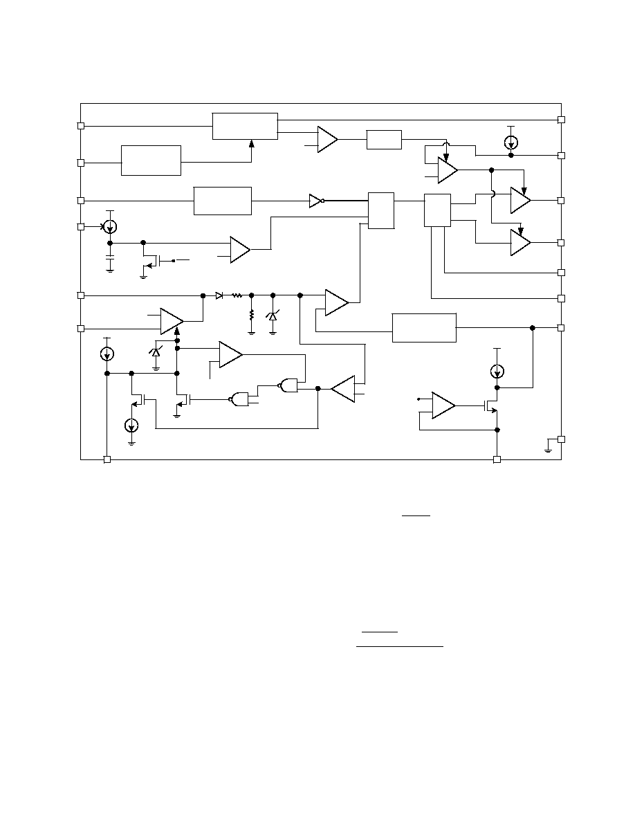
Functional Block Diagram
High Voltage
startup regulator
VIN
REF
UVLO
Bandgap
reference
+
-
1.135V
RT
Oscillator
S
Q
R
VS
+
-
1.135V
pwm
Comp
+
eAmp
1.135V
0.6V
+
-
GATE
VDD
driver
FB
Delay
Logic
AGATE
DT1
DT2
100ns blanking
CS
+
-
3.85V
UVLO
SS
GND
+
-
0.6V
+
-
ramp
SC
R
POR
+
-
1.135V
5.45V
Functional Description
HIGH VOLTAGE REGULATOR
When DC voltage from 12 to 250V is applied to the V
IN
pin, an
internal high voltage linear regulator provides a regulated output
voltage of 9.3V at the V
DD
pin. This voltage can be used to start the
DC/DC converter. Applying external voltage to the V
DD
pin that is
higher than its output voltage will disable the regulator. Therefore,
the V
IN
pin will draw negligible current once the DC/DC converter
has started, and a "bootstrap" voltage has developed at the V
DD
pin. Alternatively, the high voltage regulator can continuously
supply bias current up to 20mA powering the gate driver and all
internal circuits of HV9608. The need for a bootstrap power supply
would be eliminated in this case. However, caution must be taken
to maintain the HV9608 within its package power dissipation limits.
The output of the linear regulator is equipped with an under voltage
protection comparator that disables all internal circuits when the
voltage at the V
DD
pin falls below 7.62V. Hysteresis of 0.76V is
provided.
INPUT UNDER VOLTAGE LOCKOUT (UVLO)
The HV9608 provides a programmable under voltage protection
input (UVLO pin) that allows independent setting of the turn-on and
the turn-off limits for the input voltage of the DC/DC converter.
When the voltage applied to the UVLO pin exceeds 1.135V, the
gate driver and the reference voltage at the V
REF
pin are enabled,
and the DC/DC converter starts switching. At the same time, a
current of 14µA is sourced from the UVLO pin. This current sets
the hysteresis that can be calculated in accordance with the
following equation:
1
2
1
2
14
UVLO
R R
V
A
R
R
µ
=
+
,
where R
1
and R
2
are the input voltage divider resistors.
OSCILLATOR FREQUENCY
The switching frequency of the HV9608 can be programmed using
a single resistor connected to the R
T
pin:
[ ]
[ ]
9
1
300 10
OSC
T
T
F
Hz
R
C F
-
-
=
SOFT START
As soon as the voltage at the V
DD
pin exceeds the turn-on
threshold, a 7µA current is sourced from the SS pin into an
external soft-start capacitor C
SS
. As the voltage across C
SS
ramps
up linearly, the output of the error amplifier (COMP) gradually
increases until regulation of the output voltage is achieved. Sizing
C
SS
programs the time duration of the soft start mode. When C
SS
is
sized properly, no overshoot of the output voltage or excessive
input inrush current will occur. When the voltage at the V
DD
pin falls
below the under voltage protection threshold, C
SS
is rapidly
discharged to zero.
HV9608
6
A122104
SLOPE COMPENSATION
The HV9608 PWM controller uses an internal slope compensation
scheme that is externally programmable by appropriately selecting
two resistors R
SC1
and R
CS2
. The slope compensation ramp
generated at the CS pin can be calculated as:
[
]
[ ]
1
2
6
10
7
5
SC
SC
OSC
SC
R
R
Hz
F
.
s
/
V
m
=
-
µ
R
SC1
must be selected greater than 5 k
.
When a current sense RC filter is needed at the SC pin, the value
of R
CS2
will be dictated by the filter capacitor and the corner
frequency of the filter. The filter capacitor externally connected to
the CS pin is discharged prior to each switching cycle. It is not
recommended to use a capacitor larger than 220pF for this reason.
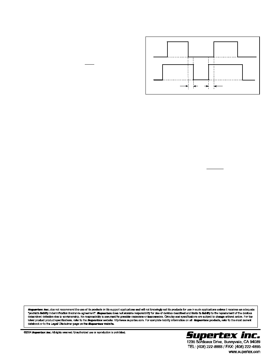
GATE DRIVE OUTPUTS
The HV9608 provides two gate-drive outputs that are configured
for driving a low-side clamp DC-DC converter, having a main
switching N-channel MOSFET (Q
1
) and an auxiliary active clamp
P-channel MOSFET (Q
2
). The GATE output is designed to drive
the main N-channel MOSFET Q
1
, while the AGATE output drives
Q
2
via a negative output charge pump circuit C
4
, D
1
, R
5
. Delays
between the leading and the trailing edges of the gate drive
outputs can be programmed using external resistors R
DT1
and R
DT2
connected to the DT1 and DT2 pins, respectively. The values of
R
DT1
and R
DT2
can be calculated according to the following
equations:
[ ]
s
d
R
DT
1
11
1
10
8
◊
=
,
[ ]
s
d
R
DT
2
11
2
10
8
◊
=
,
where d
1
is the leading edge delay, d
2
is the trailing edge delay.
(Refer to Fig. 2.)
d1
d
2
GATE
AGATE
Figure 2. Gate Drive Output timing diagram.
VOLT-SECOND CLAMP
The duty cycle of the active DC-DC converter may become very
large during load transients. This condition may cause saturation of
the power transformer or excessive voltage stress at the clamp
capacitor C
3
, potentially damaging for all switching devices. In
order to prevent this condition, the HV9608 includes a volt-second
clamp circuit that can be programmed to limit the maximum duty
cycle of the PWM controller, which is inversely proportional to the
input voltage of the DC-DC converter. The maximum duty cycle
D
MAX
is set by merely connecting a single resistor R
VS
between the
positive input terminal of the converter and the VS pin. R
VS
can be
calculated with the following equation.
[ ]
(
)
[ ]
[ ]
9
8
1
1.72 10
0.7
2 10
MAX
VS
IN
OSC
D
R
V V
d s
F
Hz
-
=
◊
-
+
+ ◊
Doc. #: DSFP-HV9608
A122104