 | –≠–ª–µ–∫—Ç—Ä–æ–Ω–Ω—ã–π –∫–æ–º–ø–æ–Ω–µ–Ω—Ç: HV9901P | –°–∫–∞—á–∞—Ç—å:  PDF PDF  ZIP ZIP |
1
HV9901
HV9901
Preliminary
06/25/02
Supertex Inc. does not recommend the use of its products in life support applications and will not knowingly sell its products for use in such applications unless it receives an adequate "products liability
indemnification insurance agreement." Supertex does not assume responsibility for use of devices described and limits its liability to the replacement of devices determined to be defective due to
workmanship. No responsibility is assumed for possible omissions or inaccuracies. Circuitry and specifications are subject to change without notice. For the latest product specifications, refer to the
Supertex website: http://www.supertex.com. For complete liability information on all Supertex products, refer to the most current databook or to the Legal/Disclaimer page on the Supertex website.
Universal Relay Driver
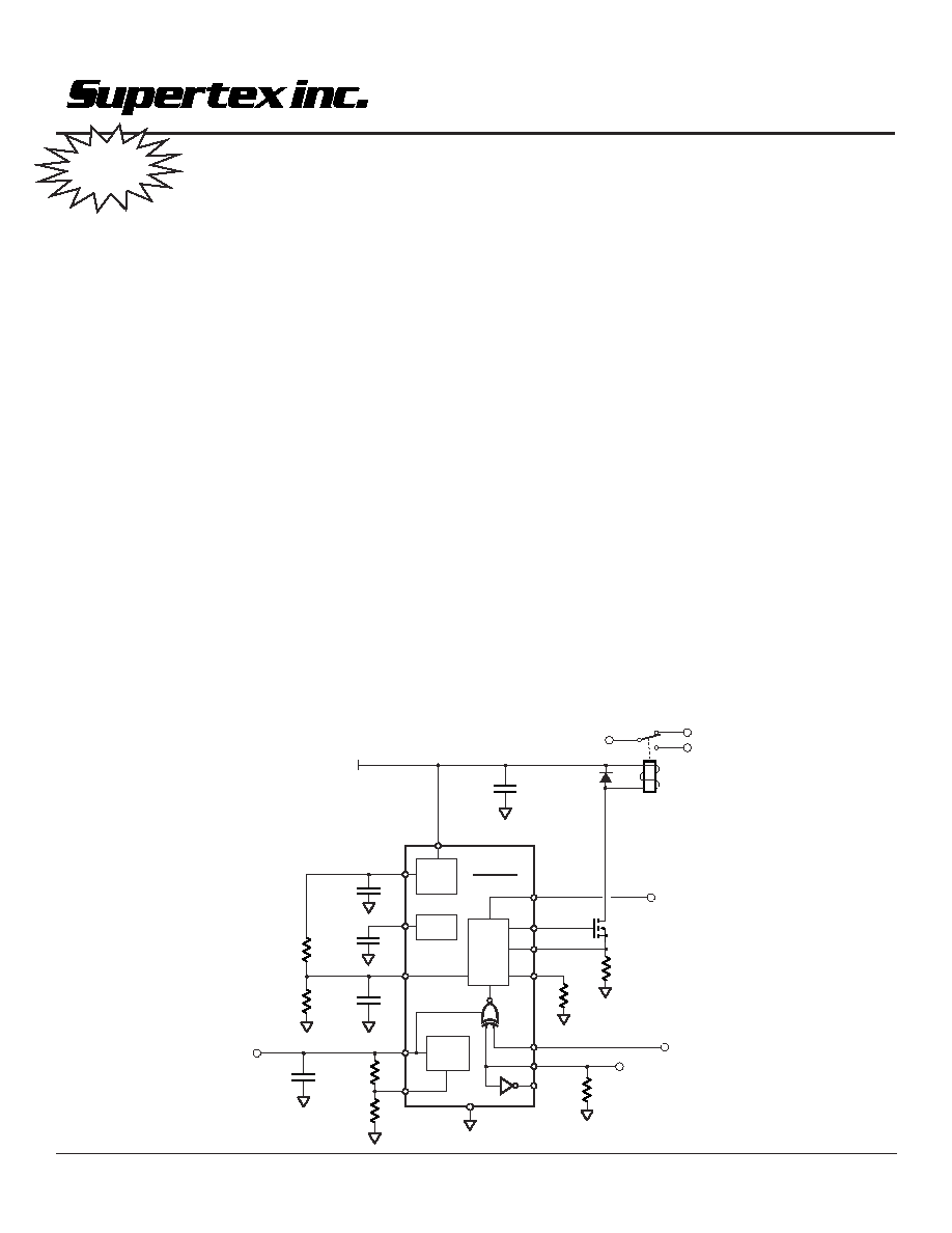
General Description
The Supertex HV9901 is a BiCMOS/DMOS universal relay
driver that employs PWM switching techniques. It is designed for
efficient and energy-saving operation of a low voltage relay with
supply voltages ranging from 8 to 450V DC through utilization of
the relay coils' inductance.
The circuit is capable of operating over a wide input voltage
range without requiring a change of any external components.
For example, this will enable users to use 5V coil relays for DC
voltages 8 - 450V or AC voltages up to 240V.
The HV9901 has an internal high-voltage regulator to power
internal PWM circuitry. Additionally it includes an adjustable
auxiliary regulator with a 1mA capability that can be used to
supply low power microcontrollers.
The pull-in current, pull-in time and hold current are all program-
mable using only two resistors and a capacitor. The PWM
switching frequency can be either
≠ Synchronized to an external clock, or
≠ Synchronized to other HV9901s, where the synchronized
frequency is the highest free-running frequency
The enable (ENI) logic input is used to turn the relay on/off.
Enable polarity may be selected via the POL input. Audible noise
is prevented using fixed switching frequencies above 20kHz.
WARNING!!!
Galvanic isolation is not provided. Dangerous voltages are
present when connected to the AC line. It is the responsibility of the designer
to ensure adequate safeguards are in place to protect the end user from
electrical shock.
Features
8V to 450V Input Voltage Range
Energy Saving Hold Current Mode
Adjustable Microcontroller Supply
Low Supply Current <1mA
Constant Current Coil Drive
Programmable Pull-in Current, Pull-in Time, and Hold
Current
Efficient PWM Operation Using the Relay Coils' Inductance
Applications
Industrial Controls
Relay Timers
White Goods
Solenoid Drivers
Home Automation
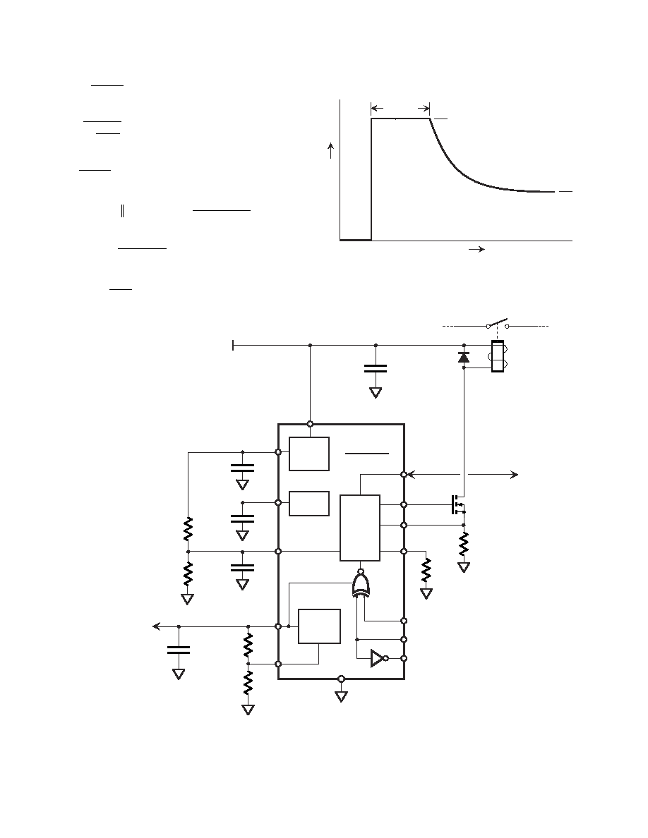
Typical Application Circuit
V
REF
A u x
Reg
PWM
Int
Reg
SYNC
GT
CS
RT
VIN
ENI
POL
ENO
FB
H/D
VREF
VDD
VCC
Enable polarity
SYNC
Enable
V
CC
V
IN
HV9901
Demo Kit
Available
2
HV9901
Electrical Characteristics
(T
A
= 25
∞
C, unless otherwise specified)
Symbol Parameters
Min
Typ
Max
Unit
Conditions
Adjustable Regulator
V
CC
Regulator Output Voltage Range
2.0
5.5
V
I
CC
=1.0mA load
I
CC
Regulator Output Current
0
1.0
mA
no load at V
DD
, See Note
V
FB
Feed Back Voltage
0
V
REF
V
DD
-1.0V
V
I
FB
Input Bias Current
25
100
nA
V
FB
= V
REF
Note: Maximum allowable load current limited by power dissipation and operating ambient temperature.
Reference
(T
A
=25
∞
C unless otherwise noted)
V
REF
Bandgap Reference Voltage
1.22
1.25
1.28
V
T
A
= 25
∞
C
V
REF
Bandgap Reference Voltage
1.20
1.25
1.30
V
T
A
= -40
∞
C to +85
∞
C
V
REF
Load Regulation
7.0
mV
0mA < I
REF
< 0.3mA
V
REF
Line Regulation
2.0
5.0
mV
6V < V
DD
< 8V
I
REF(SHORT)
Short Circuit Current
1.0
mA
I
REF(SINK)
Reference Voltage Sink Current
20
µ
A
High Voltage Regulator
8.0
450
V
I
CC
= 0.25mA load
V
IN
Input Voltage
10
450
V
I
CC
= 1.0mA load
I
IN
Supply Current
2.0
mA
no load at V
DD,
load at I
CC
=1mA,
C
GT
= 500pF, f
OSC
= 25 KHz
V
DD
Regulator Output Voltage
7.0
7.5
7.8
V
no load at V
DD,
load at
I
CC
=1mA, C
GT
= 500pF,
f
OSC
= 25 KHz
V
UVLO
V
DD
Under Voltage Lockout
6.4
6.7
7.0
V
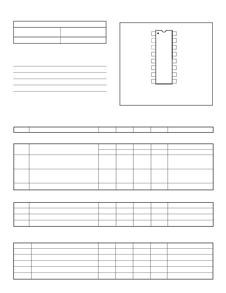
Ordering Information
Package Options
16 Lead
16 Lead
Plastic DIP
Plastic SO
HV9901P
HV9901NG
Absolute Maximum Ratings
Input voltage, V
IN
2
-0.5 to +470V
Input voltage to any other pin
2
-0.3V to V
DD
+0.3V
Continuous total power dissipation for DIP
1000 mW
1
Continuous total power dissipation for SO
750 mW
1
Operating Temperature Range
-40 to +85
∞
C
Note 1: For operation above 25
∞
C ambient derate linearly at 7.5 mW/
∞
C.
Note 2: All voltages are referenced to COM.
Pin Configuration
Plastic DIP ≠ Plastic SO
For SO-16 Pins 2 and 3 are removed
V
IN
GT
CS
COM
SYNC
V
DD
V
REF
HOLD/DELAY
FB
V
CC
ENI
ENO
POL
RT
HV9901
Top View
3
HV9901
Electrical Characteristics
(T
A
= 25
∞
C, unless otherwise specified)
Symbol Parameters
Min
Typ
Max
Unit
Conditions
MOSFET Driver Output
V
GTH
Gate Drive Output High
V
DD
≠ 0.3
V
I
OUT
= 10 mA
V
GTL
Gate Drive Output Low
0.3
V
I
OUT
= -10 mA
t
R
Rise Time
30
50
nsec
C
GT
= 500pF
t
F
Fall Time
30
50
nsec
C
GT
= 500pF
PWM
D
MAX
Maximum Duty Cycle
96.5
99.5
%
R
T
= 1.00M
D
MAX
Maximum Duty Cycle
86.5
97.5
%
R
T
= 225K
P
MIN
Minimum Output Pulse Width
100
200
nsec
Current Sensing
V
CS(HL)
Current Sense Voltage, high limit
0.775
0.833
0.891
V
t
DELAY(HL)
Current limit delay to GT high limit
200
250
ns
V
CS
= 0.88 Volts
I
CS
Input Bias Current
25
1000
nA
POL=LOW, ENI=LOW
V
OS
Low limit comparator input offset voltage
±
60
mV
t
DELAY(LL)
Current limit delay to GT, low limit
200
250
ns
V
CS
=0.47V, V
HOLD
=0.417V
V
HOLD/DEL
Hold/Delay output voltage
V
DD
-0.4
V
I
HOLD/DEL
(Sourcing)-100
µ
A,
POL=LOW, ENI=HIGH
I
HOLD/DEL
Hold Delay Input Bias Current
25
500
nA
POL=LOW, ENI=LOW
Oscillator
f
OSC
PWM Oscillator Frequency
20
25
35
kHz
R
T
= 1.00M
80
100
140
kHz
R
T
= 226K
Temperature Coefficient
170
ppm/
∞
C
T
A
= -40
∞
C to +85
∞
C
f
SYNC
Oscillator Sync Frequency
150
kHz
SYNC
Sync. Input/Output Sourcing Current
20
55
µ
A
SYNC
Sync. Input/Output Sinking Current
1.0
mA
V
SYNC
= 0.1V
V
SYNC
Sync Input Logic Low Voltage
1.0
V
4
HV9901
Enable Logic Truth Table
POL
ENI
ENO
Gate Drive Output
LOW
LOW
HIGH
V
GT
= Oscillating Output, Duty Cycle depends on Inductive Load
LOW
HIGH
LOW
V
GT
= LOW, SYNC = HIGH, Oscillator shut down.
HIGH
HIGH
LOW
V
GT
= Oscillating Output, Duty Cycle depends on Inductive Load
HIGH
LOW
HIGH
V
GT
= LOW, SYNC = HIGH, Oscillator shut down.
Electrical Characteristics, continued
(T
A
= 25
∞
C, unless otherwise specified)
Symbol Parameters
Min
Typ
Max
Unit
Conditions
Enable Logic
t
ENI
Shutdown Delay
50
100
nsec
2V < V
CC
< 5.5V
V
ENI
Enable Input Voltage - High
0.7V
CC
V
CC
V
2V < V
CC
< 5.5V
V
ENI
Enable Input Voltage - Low
0
0.3V
CC
V
2V < V
CC
< 5.5V
I
ENI
Enable Input Current - High
1.0
5.0
µ
A
2V < V
CC
< 5.5V
I
ENI
Enable Input Current - Low
-5.0
-1.0
µ
A
2V < V
CC
< 5.5V
V
POL
Polarity Voltage - High
0.7V
CC
V
CC
V
2V < V
CC
< 5.5V
V
POL
Polarity Voltage - Low
0
0.3V
CC
V
2V < V
CC
< 5.5V
I
POL
Polarity Current - High
1.0
5.0
µ
A
2V < V
CC
< 5.5V
I
POL
Polarity Current - Low
-5.0
-1.0
µ
A
2V < V
CC
< 5.5V
V
ENO
Enable Output Voltage - High
0.9V
CC
V
CC
V
2V < V
CC
< 5.5V
V
ENO
Enable Output Voltage - Low
0
0.1V
CC
V
2V < V
CC
< 5.5V
5
HV9901
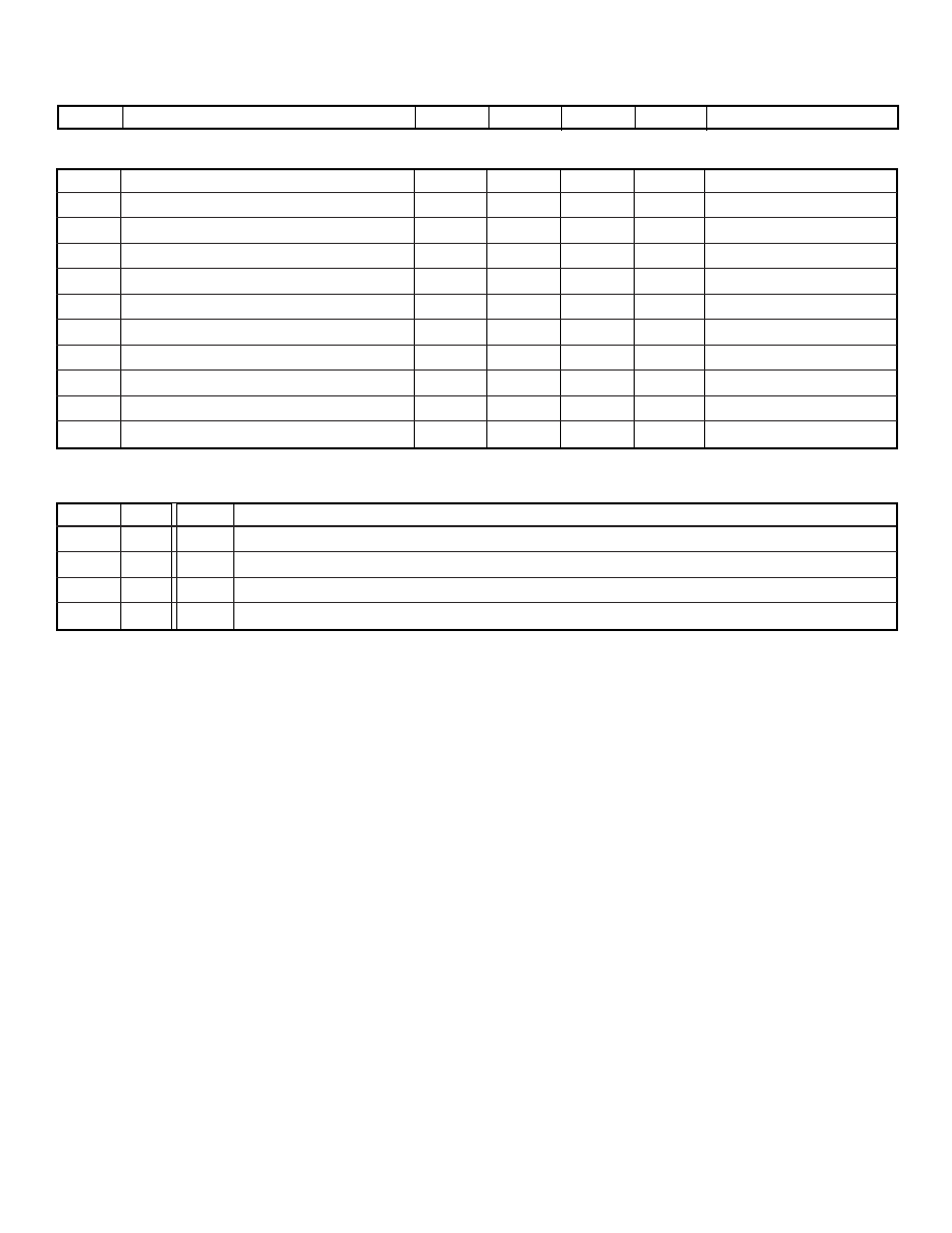
Applications Information
I
PULL-IN
t
PULL-IN
I
HOLD
Time
Current
V
REF
PWM
SYNC
GT
CS
RT
VIN
ENI
POL
ENO
FB
H/D
VREF
VDD
VCC
2.0≠5.5V
@ 1mA
V
IN
R
SENSE
R
OSC
R
HDb
R
HDa
C
REF
C
DD
C
IN
Q
SW
R
FBa
R
FBb
A u x
Reg
Int
Reg
HV9901
C
HD
I
V
R
V
V
V
R
R
V
I
V
R
t
R
R
C
V
V
V
V
f
R
V
R
PULL IN
CS HL
SENSE
CS HI
CS LL
DD
HD
HD
DD
HOLD
CS LL
SENSE
PULL IN
HDa
HDb
HD
CS HL
DD
CS LL
DD
PWM
OSC
CC
FBa
-
-
=
=
=
+
=
=
= -
(
)
-
-
-
+
=
+
(
)
(
)
(
)
(
)
(
)
(
)
ln
833mV nom
7.5V nom
3.23kHz
21.8GHz
1.25V
1
1
1
9
6
(valid for f
> 23kHz)
pwm
R
R
FBb
6
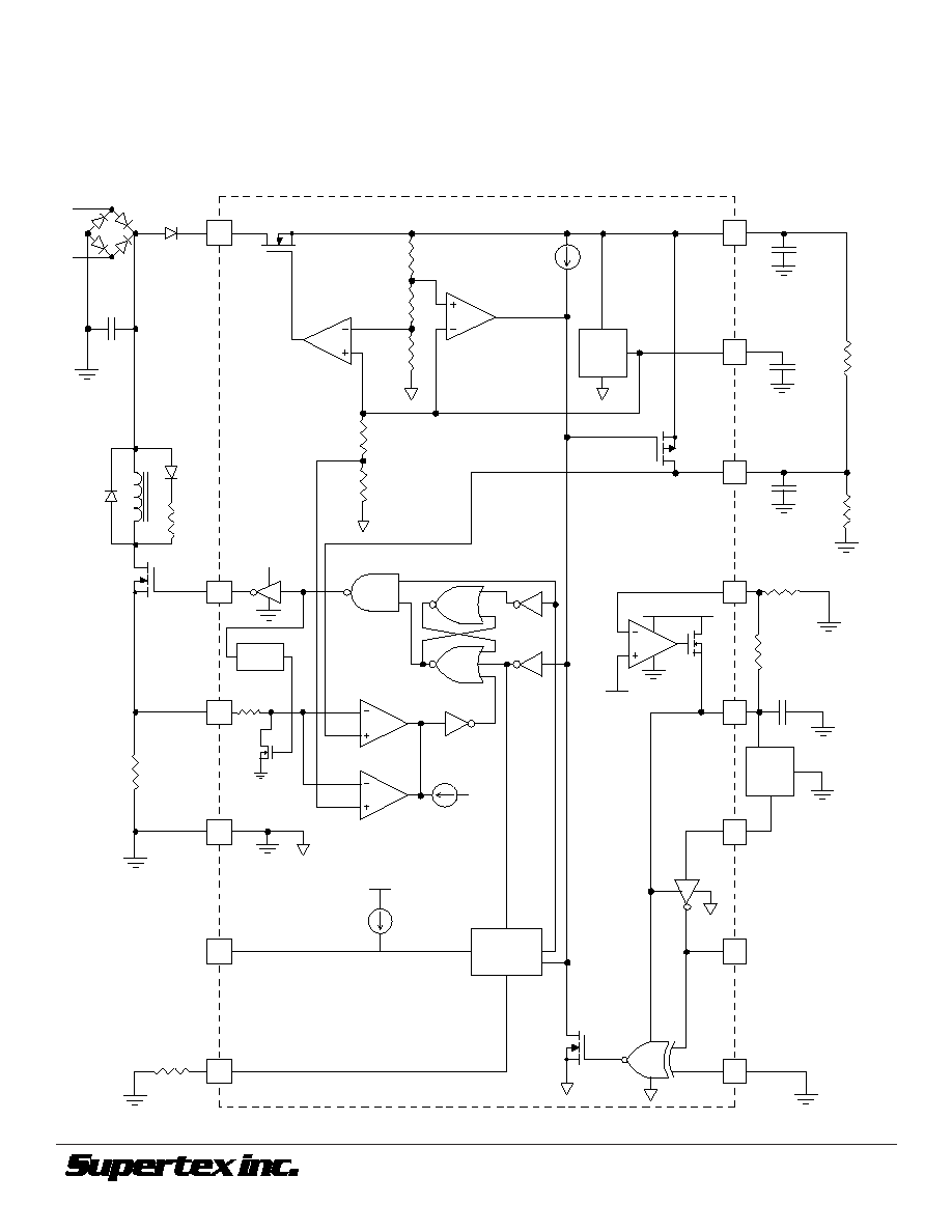
HV9901
Functional Block Diagram and Typical Application
1235 Bordeaux Drive, Sunnyvale, CA 94089
TEL: (408) 744-0100 ∑ FAX: (408) 222-4895
www.supertex.com
06/26/02rev.4
©2002 Supertex Inc. All rights reserved. Unauthorized use or reproduction prohibited.
VIN
1N4148
A
RS
100nF
UVLO
C
See Note 1.
VREF
VDD
100nF
4.7
µ
F
R
S
R
CS
GT
1N4937
RELA
Y
VN2460N8
LED
10K
Bandgap
Reference
1.25 V
COM
Q
VDD
Oscillator
shut down
SYNC
Rosc
RT
ENI
ENO
POL
VCC
µ
P
100nF
5 V
RFBa
RFBb
FB
HOLD/DELAY
RHDb
RHDa
4
5
6
7
8
9
10
11
12
13
14
15
16
CHD
C
C
High Limit
Low Limit
VDD
100ns
Delay
R
2R
1.25V
VDD
High Duty
Cycle
Oscillator
Notes: 1. This diode and bridge rectifier required only for AC operation.
2. For non-isolated AC operation the entire circuit must be floating.
3. All comparators have open drain outputs.
1
VDD
40
µ
A
5.5k