HV9910
1
C110504
Features
>90% Efficiency
8V to 450V input range
Constant-current LED driver
Applications from a few mA to more than 1A
Output
LED string from one to hundreds of diodes
PWM Low-Frequency Dimming via Enable pin
Input Voltage Surge ratings up to 450V
Applications
DC/DC or AC/DC LED Driver applications
RGB Backlighting LED Driver
Back Lighting of Flat Panel Displays
General purpose constant current source
Signage and Decorative LED Lighting
Automotive
Chargers
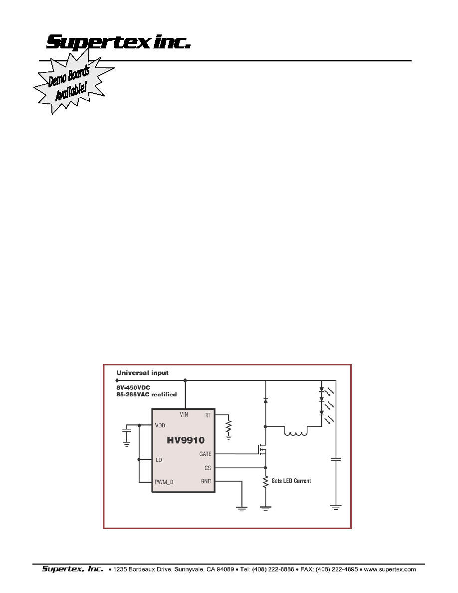
Typical Application
Description
The HV9910 is a PWM high-efficiency LED driver
control IC. It allows efficient operation of High
Brightness (HB) LEDs from voltage sources
ranging from 8VDC up to 450VDC. The HV9910
controls an external MOSFET at fixed switching
frequency up to 300kHz. The frequency can be
programmed using a single resistor. The LED string
is driven at constant current rather than constant
voltage, thus providing constant light output and
enhanced reliability. The output current can be
programmed between a few milliamps and up to
more than 1.0A.
HV9910 uses a rugged high voltage junction
isolated process that can withstand an input voltage
surge of up to 450V. Output current to an LED
string can be programmed to any value between
zero and its maximum value by applying an
external control voltage at the linear dimming
control input of the HV9910. The HV9910 provides
a low-frequency PWM dimming input that can
accept an external control signal with a duty ratio of
0-100% and a frequency of up to a few kilohertz.
Universal High Brightness LED Driver
C110504
HV9910
2
C110504
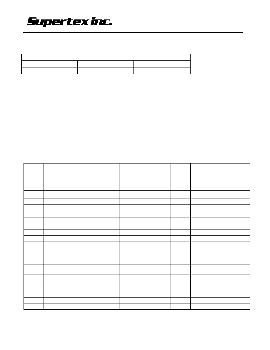
Ordering Information
Absolute Maximum Ratings
V
IN
to GND ...............................................................-0.5V to +470V
CS...............................................................-0.3V to Vdd + 0.3V
LD, PWM_D to GND........................................-0.3V to (Vdd ---0.3V)
GATE to GND ................................................-0.3V to (Vdd
+ 0.3V)
V
DDMAX
..........................................................................13.5V
Continuous Power Dissipation (T
A
= +25�C) (Note 1)
16-Pin SO (derate 7.5mW/�C above +25�C)......................750mW
8-Pin DIP (derate 9mW/�C above +25�C)..........................900mW
8-Pin SO (derate 6.3mW/�C above +25�C)........................630mW
Operating Temperature Range ...............................-40�C to +85�C
Junction Temperature..........................................................+125�C
Storage Temperature Range ................................-65�C to +150�C
Stresses beyond those listed under ``Absolute Maximum Ratings'' may cause permanent damage to the device. These are stress ratings only, and functional
operation of the device at these or any other conditions beyond those indicated in the operational sections of the specifications is not implied. Exposure to
absolute maximum rating conditions for extended periods may affect device reliability.
Specifications
(T
A
= 25�C unless noted otherwise)
Symbol Description
Min
Typ Max Units Conditions
V
INDC
Input DC supply voltage range
8.0
450
V
DC input voltage
I
INsd
Shut-Down mode supply current
0.5
1
mA
Pin PWM_D to GND, V
IN
= 8V
V
DD
Internally regulated voltage
7.0
7.5
8.0
V
V
IN
= 8�450V, I
DD(ext)
=0, pin Gate
open
V
DDmax
Maximal pin Vdd voltage
13.5
V
When an external voltage applied
to pin Vdd
I
DD(ext)
V
DD
current available for external circuitry
1
1.0
mA
V
IN
= 8�100V
UVLO V
DD
undervoltage lockout threshold
6.45
6.7
6.95
V
Vin rising
UVLO
V
DD
undervoltage lockout hysteresis
500
mV
Vin falling
V
EN(lo)
Pin PWM_D input low voltage
1.0
V
V
IN
= 8�450V
V
EN(hi)
Pin PWM_D input high voltage
2.4
V
V
IN
= 8�450V
R
EN
Pin PWM_D pull-down resistance
50
100
150
k
V
EN
= 5V
V
CS(hi)
Current sense pull-in threshold voltage
225
250
275
mV
@TA = -40
�
C to +85
�
C
V
GATE(hi)
GATE high output voltage
V
DD
-0.3 V
DD
V
I
OUT
= 10mA
V
GATE(lo)
GATE low output voltage
0
0.3
V
I
OUT
= -10mA
f
OSC
Oscillator
frequency
20
80
25
100
30
120
kHz
kHz
R
OSC
= 1.00M
R
OSC
= 226k
D
MAXhf
Maximum Oscillator PWM Duty Cycle
100
%
F
PWMhf
= 25kHz, at GATE, CS to
GND. GBD
V
LD
Linear Dimming pin voltage range
0
250
mV
@TA = <85
�
C, Vin = 12V
T
BLANK
Current sense blanking interval
150 215
280 ns V
CS
= 0.55V
LD
, V
LD
= V
DD
t
DELAY
Delay from CS trip to GATE lo
300
ns
Vin = 12V, V
LD
= 0.15, V
CS
= 0 to
0.22V after T
BLANK
t
RISE
GATE output rise time
30
50
ns
C
GATE
= 500pF
t
FALL
GATE output fall time
30
50
ns
C
GATE
= 500pF
1
Also limited by package power dissipation limit, whichever is lower.
Package Options
SO-16 DIP-8 SO-8
HV9910NG HV9910P HV9910LG
HV9910
3
C110504
Pinout
No Connects (NC) are not internally connected and may be used for pass-thru PCB traces.
Block Diagram & Typical Application
Description
Name
SO-16 SO-8
DIP-8
V
IN
1
1
Input voltage 8V to 450V DC
CS
4
2
Senses LED string current
GND
5
3
Device ground
GATE
8
4
Drives the gate of the external MOSFET
PWM_D
9
5
Low Frequency PWM Dimming pin, also Enable
input. Internal 100k
pull-down to GND
V
DD
12
6
Internally regulated supply voltage. 7.5V
nominal. Can supply up to 1mA for external
circuitry. A sufficient storage capacitor is used to
provide storage when the rectified AC input is
near the zero crossings.
LD
13
7
Linear Dimming by changing the current limit
threshold at current sense comparator
R
OSC
14
8
Oscillator control. A resistor connected between
this pin and ground sets the PWM frequency.
16-Pin SOIC
8-Pin DIP/SOIC

HV9910
4
C110504
Application Information
AC/DC Off-Line Applications
The HV9910 is a low-cost off-line buck, boost or
buck-boost converter control IC specifically
designed for driving multi-LED stings or arrays. It
can be operated from either universal AC line or
any DC voltage between 8-450V. Optionally, a
passive power factor correction circuit can be used
in order to pass the AC harmonic limits set by EN
61000-3-2 Class C for lighting equipment having
input power less than 25W. The HV9910 can drive
up to hundreds of High-Brightness (HB) LEDs or
multiple strings of HB LEDs. The LED arrays can
be configured as a series or series/parallel
connection. The HV9910 regulates constant current
that ensures controlled brightness and spectrum of
the LEDs, and extends their lifetime. The HV9910
features an enable pin (PWM_D) that allows PWM
control of brightness.
The HV9910 can also control brightness of LEDs
by programming continuous output current of the
LED driver (so-called linear dimming) when a
control voltage is applied to the LD pin.
The HV9910 is offered in standard 8-pin SOIC and
DIP packages. It is also available in a high voltage
rated SO-16 package for applications that require
V
IN
greater than 250V.
The HV9910 includes an internal high-voltage
linear regulator that powers all internal circuits and
can also serve as a bias supply for low voltage
external circuitry.
LED Driver Operation
The HV9910 can control all basic types of
converters, isolated or non-isolated, operating in
continuous or discontinuous conduction mode.
When the gate signal enhances the external power
MOSFET, the LED driver stores the input energy in
an inductor or in the primary inductance of a
transformer and, depending on the converter type,
may partially deliver the energy directly to LEDs
The energy stored in the magnetic component is
further delivered to the output during the off-cycle of
the power MOSFET producing current through the
string of LEDs (Flyback mode of operation).
When the voltage at the V
DD
pin exceeds the UVLO
threshold the gate drive is enabled. The output
current is controlled by means of limiting peak
current in the external power MOSFET. A current
sense resistor is connected in series with the
source terminal of the MOSFET. The voltage from
the sense resistor is applied to the CS pin of the
HV9910. When the voltage at CS pin exceeds a
peak current sense voltage threshold, the gate
drive signal terminates, and the power MOSFET
turns off. The threshold is internally set to 250mV,
or it can be programmed externally by applying
voltage to the LD pin. When soft start is required, a
capacitor can be connected to the LD pin to allow
this voltage to ramp at a desired rate, therefore,
assuring that output current of the LED ramps
gradually.
Optionally, a simple passive power factor correction
circuit, consisting of 3 diodes and 2 capacitors, can
be added as shown in the application circuit
diagram of Figure 1.
Supply Current
A current of 1mA is needed to start the HV9910. As
shown in block diagram, this current is internally
generated in HV9910 without using bulky startup
resistors typically required in the offline
applications. Moreover, in many applications the
HV9910 can be continuously powered using its
internal linear regulator that provides a regulated
voltage of 7.5V for all internal circuits.
Setting Light Output
When the buck converter topology of Figure 1 is
selected, the peak CS voltage is a good
representation of the average current in the LED.
However, there is a certain error associated with
this current sensing method that needs to be
accounted for. This error is introduced by the
difference between the peak and the average
current in the inductor. For example if the peak-to-
peak ripple current in the inductor is 150mA, to get
a 500mA LED current, the sense resistor should be
250mV/(500mA+ 0.5*150mA)=0.43
.
Dimming
Dimming can be accomplished in two ways,
separately or combined, depending on the
application. Light output of the LED can be
controlled either by linear change of its current, or
by switching the current on and off while
maintaining it constant. The second dimming
method (so-called PWM dimming) controls the LED
brightness by varying the duty ratio of the output
current.
The linear dimming can be implemented by
applying a control voltage from 0 to 250mV to the
LD pin. This control voltage overrides the internally
set 250mV threshold level of the CS pin and
programs the output current accordingly. For
HV9910
5
C110504
example, a potentiometer connected between V
DD
and ground can program the control voltage at the
CS pin. Applying a control voltage higher than
250mV will not change the output current setting.
When higher current is desired, select a smaller
sense resistor.
The PWM dimming scheme can be implemented by
applying an external PWM signal to the PWM_D
pin. The PWM signal can be generated by a
microcontroller or a pulse generator with a duty
cycle proportional to the amount of desired light
output. This signal enables and disables the
converter modulating the LED current in the PWM
fashion. In this mode, LED current can be in one of
the two states: zero or the nominal current set by
the current sense resistor. It is not possible to use
this method to achieve average brightness levels
higher than the one set by the current sense
threshold level of the HV9910. By using the PWM
control method of the HV9910, the light output can
be adjusted between zero and 100%. The accuracy
of the PWM dimming method is limited only by the
minimum gate pulse width, which is a fraction of a
percent of the low frequency duty cycle.
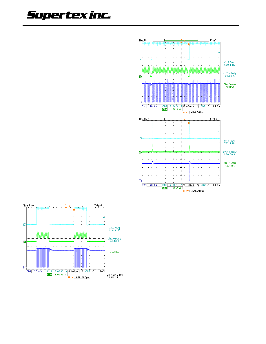
Some of the typical waveforms illustrating the PWM
dimming method used with the application circuit of
Figure 1 are given below. CH
1
shows the MOSFET
Drain voltage, CH
2
is the PWM signal to pin
PWM_D and CH
4
is the current in the LED string.
95% PWM Ratio at 500Hz Dimming
0.4% PWM Ratio at 500Hz Dimming
Programming Operating Frequency
The operating frequency of the oscillator is
programmed between 25 and 300kHz using an
external resistor connected to the R
OSC
pin:
F
OSC
= 25000/(R
OSC
[k
] + 22) [kHz]
Power Factor Correction
When the input power to the LED driver does not
exceed 25W, a simple passive power factor
correction circuit can be added to the HV9910
application circuit of Figure 1 in order to pass the
AC line harmonic limits of the EN61000-3-2
standard for Class C equipment. The typical
application circuit diagram shows how this can be
done without affecting the rest of the circuit
significantly. A simple circuit consisting of 3 diodes
and 2 capacitors is added across the rectified AC
line input to improve the line current harmonic
distortion and to achieve a power factor greater
than 0.85.
33% PWM Ratio at 500Hz Dimming