HV9911
1
NR011206
Initial Release
Features
Switch mode controller for single switch drivers
o
Buck
o
Boost
o
Buck-boost
Works with high side current sensing
Closed loop control of output current
High PWM dimming ratio
Internal 9 to 250V linear regulator (can be extended
using external zener diodes)
Internal 2% Voltage Reference (-40∞C<T
A
<85∞C)
Constant frequency or constant off-time operation
Programmable slope compensation
Enable & PWM dimming
+0.25A/-0.5A gate drive (V
DD
= 10V)
Output short circuit protection
Output over voltage protection
Synchronization capability
Programmable MOSFET current limit
Soft start
Applications
RGB backlight applications
Automotive LED driver application
Battery Powered LED lamps
Other DC/DC LED drivers
General Description
The HV9911 is a current mode control LED driver IC designed to
control single switch PWM converters (buck, boost or buck-boost),
in a constant frequency or constant off-time mode. The controller
uses a peak current control scheme, (with programmable slope
compensation), and includes an internal transconductance amplifi er
to control the output current in closed loop, enabling high output
current accuracy (in the case of buck and buck-boost converters,
the high side output current can be sensed by using the HV7800).
In the constant frequency mode, multiple HV9911s can by
synchronized to each other, or to an external clock, using the SYNC
pin. Programmable MOSFET current limit enables current limiting
during input under voltage and output overload conditions. The IC
also includes a 0.25A source and 0.5A sink gate driver for high power
applications. An internal 9 to 250V linear regulator powers the IC,
eliminating the need for a separate power supply for the IC. HV9911
provides a TTL compatible, PWM dimming input that can accept an
external control signal with a duty ratio of 0-100% and a frequency
of up to a few kilohertz.
The HV9911 based LED driver is ideal for RGB backlight applications
with DC inputs. The HV9911 based LED Lamp drivers can achieve
effi ciency in excess of 90% for buck and boost applications.
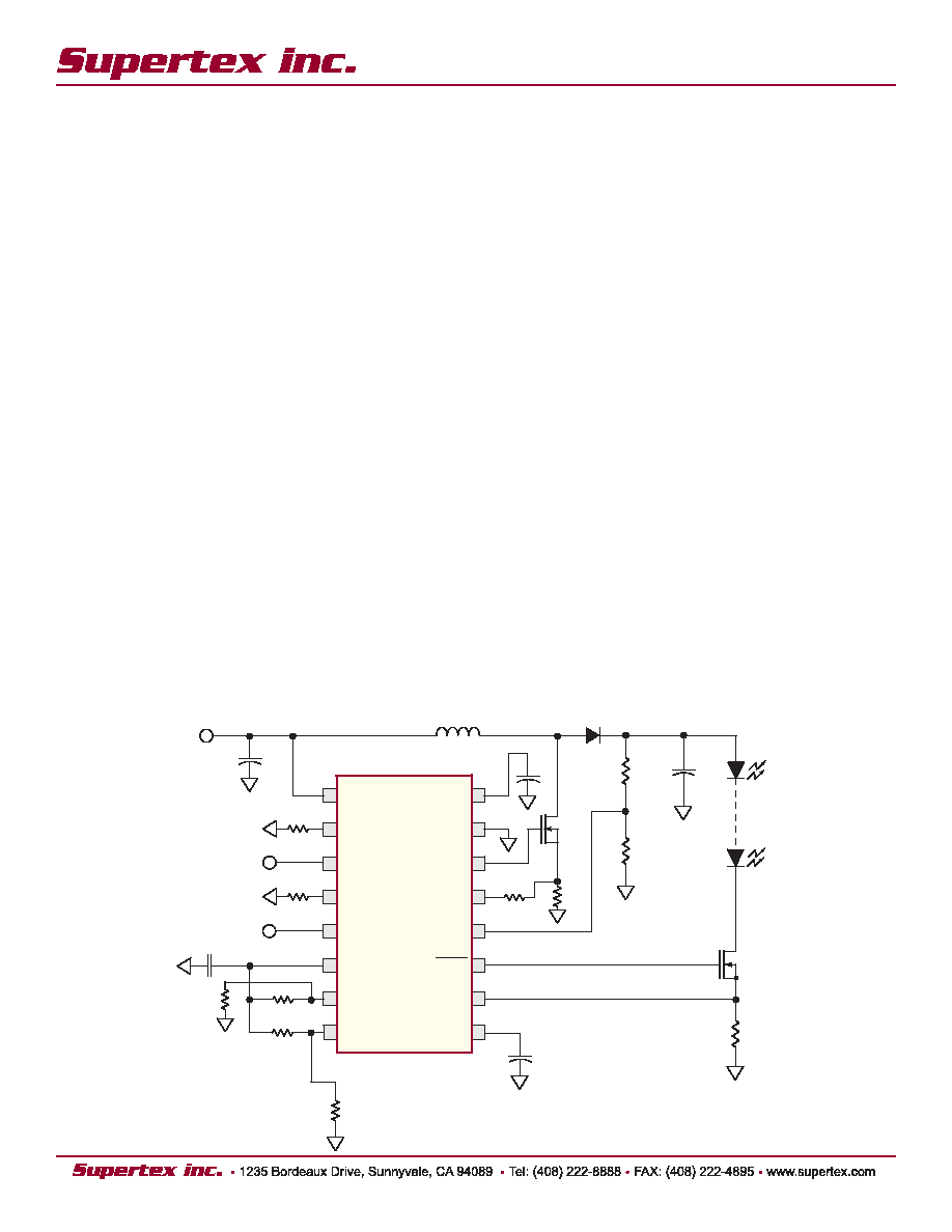
Typical Application Circuit
C
C
V
IN
R
T
R
SLOPE
C
REF
R
L1
R
L2
R
SC
R
CS
D1
C
O
R
R2
R
R1
R
S
Q
2
R
OVP2
R
OVP1
L
1
V
IN
V
DD
FDBK
FAULT
COMP
PWMD
I
REF
REF
GND
C
LIM
CS
GATE
OVP
SC
HV9911
SYNC
R
T
C
DD
C
IN
Q
1
Switch-mode LED Driver IC with High Current Accuracy
2
NR011206
HV9911
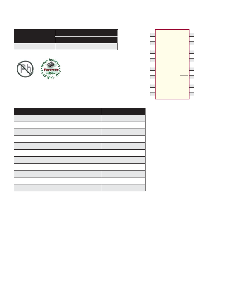
Ordering Information
DEVICE
Package Options
16-Lead SOIC
HV9911
HV9911NG-G
-G indicates package is RoHS compliant (`Green')
Absolute Maximum Ratings
Parameter
Value
V
IN
to GND
-0.5V to +250V
V
DD
to GND
-0.3V to +13.5V
CS1, CS2 to GND
-0.3V to (V
DD
+ 0.3V)
PWMD to GND
-0.3V to (V
DD
+ 0.3V)
GATE to GND
-0.3V to (V
DD
+ 0.3V)
All other pins to GND
-0.3V to (V
DD
+ 0.3V)
Continuous Power Dissipation (TA = +25∞C)
16-Pin SOIC (derate 6.3mW/∞C above +25∞C)
630mW
Operating Temperature Range
-40∞C to +85∞C
Junction Temperature
+125∞C
Storage Temperature Range
-65∞C to +150∞C
Stresses beyond those listed under "Absolute Maximum Ratings" may cause permanent damage to the
device. These are stress ratings only, and functional operation of the device at these or any other conditions
beyond those indicated in the operational sections of the specifi cations is not implied. Exposure to absolute
maximum rating conditions for extended periods may affect device reliability.
Pin Assignment
V
IN
V
DD
FDBK
FAULT
COMP
PWMD
I
REF
REF
GND
C
LIM
CS
GATE
OVP
SC
HV9911
SYNC
R
T
1
2
3
4
5
6
7
8
9
10
11
12
13
14
15
16
3
NR011206
HV9911
Symbol
Parameter
Min
Typ
Max
Units
Conditions
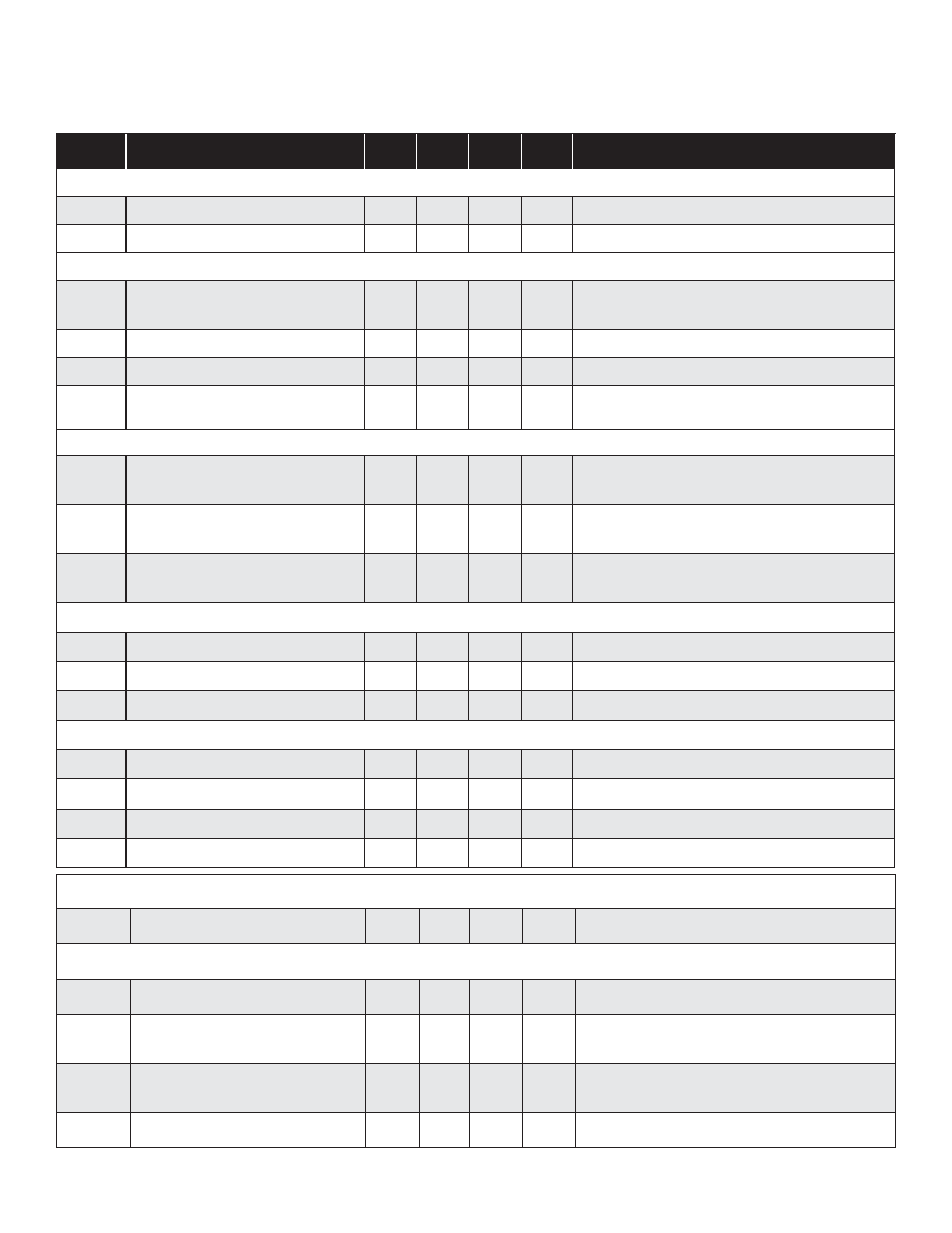
Input
V
INDC
Input DC supply voltage range*
9
-
250
V
DC input voltage
I
INSD
Shut-Down mode supply current*
-
1.0
1.5
mA
PWM_D connected to GND, V
IN
= 24V
Internal Regulator
V
DD
Internally regulated voltage*
7.25
7.75
8.25
V
V
IN
= 9≠250V, I
DD(ext)
= 0,
PWMD connected to GND
UVLO
V
DD
undervoltage lockout threshold
6.65
6.90
7.20
V
V
DD
rising
UVLO
V
DD
undervoltage lockout hysteresis
-
500
-
mV
---
V
DD(ext)
Steady State External Voltage
which can applied at the V
DD
pin
1
-
-
12
V
---
Reference
V
REF
REF pin voltage*
1.225
1.25
1.275
V
REF bypassed with a 0.1µF capacitor to GND;
I
REF
= 0; V
DD
= 7.75V; PWMD = GND
V
REFLINE
Line regulation of reference voltage
0
-
20
mV
REF bypassed with a 0.1µF capacitor to GND;
I
REF
= 0; V
DD
= 7.25 ≠ 12V; PWMD = GND
V
REFLOAD
Load regulation of reference
voltage
0
-
10
mV
REF bypassed with a 0.1µF capacitor to GND;
I
REF
= 0 - 500µA; PWMD = GND
PWM Dimming
V
PWMD(lo)
PWMD input low voltage*
-
-
0.80
V
V
DD
= 7.25V ≠ 12V
V
PWMD(hi)
PWMD input high voltage*
2.0
-
-
V
V
DD
= 7.25V ≠ 12V
R
PWMD
PWMD pull-down resistance
50
100
150
k
V
PWMD
= 5.0V
GATE
I
SOURCE
GATE short circuit current
0.2
-
-
A
V
GATE
= 0V; V
DD
= 7.75V
I
SINK
GATE sinking current
0.4
-
-
A
V
GATE
= 7.75V ; V
DD
= 7.75V
T
RISE
GATE output rise time
-
50
85
ns
C
GATE
= 1nF; V
DD
= 7.75V
T
FALL
GATE output fall time
-
25
45
ns
C
GATE
= 1nF; V
DD
= 7.75V
Over Voltage Protection
V
OVP
IC Shut down voltage*
1.215
1.25
1.285
V
V
DD
= 7.25 ≠ 12V ; OVP rising
Current Sense
T
BLANK
Leading Edge Blanking
100
-
375
ns
---
T
DELAY1
Delay to Output of OP comparator
-
-
180
ns
OP = V
DD
; C
LIM
= REF;
C
SENSE
= 0 to 600mV step
T
DELAY2
Delay to Output of C
LIMIT
comparator
-
-
180
ns
OP = V
DD
; C
LIM
= 300mV ;
C
SENSE
= 0 to 400mV step
V
OFFSET
Comparator Offset voltage
-10
-
10
mV
---
Electrical Characteristics
(Over recommended operating conditions, V
IN
= 24V, T
A
= 25∞C, unless otherwise specifi ed)

4
NR011206
HV9911
Internal Transconductance Opamp
GB
Gainbandwidth product
#
-
1.0
-
MHz
75pF capacitance at OP pin
A
V
Open Loop DC Gain
66
-
-
dB
Output Open
V
CM
Input common-mode range
#
-0.3
-
3.0
V
---
V
O
Output Voltage Range
#
0.7
-
6.75
-
V
DD
= 7.75V
g
m
Transconductance
340
435
530
µA/V
---
V
OFFSET
Input Offset Voltage
-3.0
-
3.0
mV
---
I
BIAS
Input bias current
#
-
0.5
1.0
nA
---
Oscillator
f
OSC, MIN
Minimum Oscillator frequency*
22
25
28
kHz
R
T
= 3.65M
f
OSC, MAX
Maximum Oscillator frequency*
308
350
392
kHz
R
T
= 261k
D
MAX
Maximum Duty cycle
-
90
-
%
---
I
OUTSYNC
Sync output current
-
10
20
µA
---
I
INSYNC
Sync input current
0
-
200
µA
V
SYNC
< 0.1V
Output Short Circuit
T
OFF
Propagation time for short circuit
detection
-
-
250
ns
NI=200mV ; INV=450mV;
FAULT goes from high to low
T
RISE,FAULT
Fault output rise time
-
-
300
ns
1nF capacitor at FAULT pin
T
FALL,FAULT
Fault output fall time
-
-
200
ns
1nF capacitor at FAULT pin
G
FAULT
Amplifi er gain at NI pin
1.8
2
2.2
NI=200mV
Soft Start
I
CLIM
Current into CLIM pin when pulled
low
-
-
200
µA
FAULT is low ;
6.25k resistor between REF and C
LIM
Slope Compensation
I
SLOPE
Current Sourced out of SLOPE pin
0
-
100
µA
---
G
SLOPE
Internal Current Mirror ratio
1.8
2
2.2
-
I
SLOPE
= 50µA ; RC
SENSE
= 1k
1
Parameters are not guaranteed to be within specifi cations if the external V
DD
voltage is greater than V
DD(ext)
* Specifi cations which apply over the full operating ambient temperature range of -40∞C < T
A
< +85∞C.
# Guaranteed by design
Symbol
Parameter
Min
Typ
Max
Units
Conditions
5
NR011206
HV9911
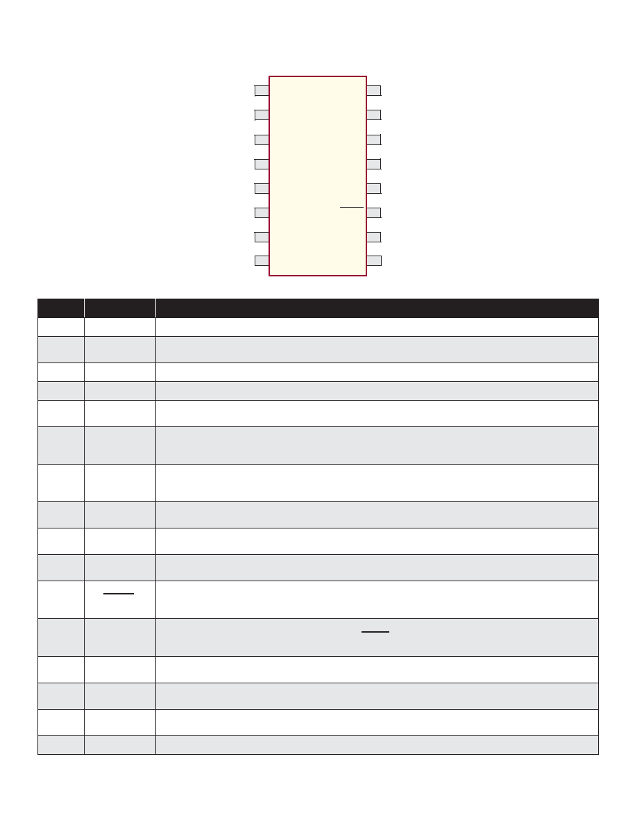
V
IN
V
DD
FDBK
FAULT
COMP
PWMD
I
REF
REF
GND
C
LIM
CS
GATE
OVP
SC
HV9911
SYNC
R
T
1
2
3
4
5
6
7
8
9
10
11
12
13
14
15
16
Pin Assignment
Pin Description
Pin #
Pin
Description
1
V
IN
This pin is the input of a 9 ≠ 250V high voltage regulator.
2
V
DD
This is a power supply pin for all internal circuits. It must be bypassed with a low ESR capacitor to GND
(at least 0.1uF).
3
GATE
This pin is the output gate driver for an external N-channel power MOSFET.
4
GND
Ground return for all circuits. This pin must be connected to the return path from the input.
5
CS
This pin is used to sense the drain current of the external power FET. It includes a built-in 100ns (min)
blanking time.
6
SC
Slope compensation for current sense. A resistor between SC and GND will program the slope
compensation. In case of constant off-time mode of operation, slope compensation is unnecessary and
the pin can be left open.
7
R
T
This pin sets the frequency or the off-time of the power circuit. A resistor between RT and GND will
program the circuit in constant frequency mode. A resistor between RT and GATE will program the circuit
in a constant off-time mode.
8
SYNC
This I/O pin may be connected to the SYNC pin of other HV9911 circuits and will cause the oscillators to
lock to the highest frequency oscillator.
9
C
LIM
This pin provides a programmable input current limit for the converter. The current limit can be set by using
a resistor divider from the REF pin. Soft start can also be provided using this pin.
10
REF
This pin provides 2% accurate reference voltage. It must be bypassed with at least a 10nF capacitor to
GND
11
FAULT
This pin is pulled to ground when there is an output short circuit condition or output over voltage condition.
This pin can be used to drive an external MOSFET in the case of boost converters to disconnect the load
from the source
12
OVP
This pin provides the over voltage protection for the converter. When the voltage at this pin exceeds 1.25V,
the gate output of the HV9912 is turned off and FAULT goes low. The IC will turn on when the power is
recycled
13
PWMD
When this pin is pulled to GND (or left open), switching of the HV9911 is disabled. When an external TTL
high level is applied to it, switching will resume
14
COMP
Stable Closed loop control can be accomplished by connecting a compensation network between COMP
and GND
15
I
REF
The voltage at this pin sets the output current level. The current reference can be set using a resistor
divider from the REF pin
16
FDBK
This pin provides output current feedback to the HV9911 by using a current sense resistor

6
NR011206
HV9911
Functional Block Diagram
Functional Description
Vbg
V
IN
V
DD
REF
GATE
+
_
+
_
13R
R
FDBK
IREF
COMP
GND
PWMD
POR
R
T
SYNC
S
R
Q
Gm
+
_
C
LIM
100ns
Blanking
+
_
2
CS
SS
SC
+
_
ramp
1:2
SS
+
_
Vbg
OVP
R
S
Q
FAULT
POR
SS
Q
One Shot
Linear Regulator
Continuous mode buck and boost converters are ideal as
LED drivers, as they can achieve high effi ciencies greater
than 90%. The HV9911 is a switch-mode converter LED
driver designed to control a continuous conduction mode
buck or boost in a constant frequency (or constant off-time)
mode. The IC includes an internal linear regulator, which
operates from input voltages of 9V to 250V eliminating the
need for an external power supply for the IC. The IC includes
features typically required in LED drivers like open LED
protection, output short circuit protection, linear and PWM
dimming, programmable input current limiting and accurate
control of the LED current. A high current gate drive output
enables the controller to be used in high power converters.
Linear Regulator
The built in linear regulator operates from input voltages of
9V to 250V and provides a 7.75V voltage at the V
DD
pin. This
7.75V is used to power the IC and also provide the power to
external circuits connected at the V
DD
and VREF pins. This
linear regulator can be turned off by overdriving the V
DD
pin
using an external bootstrap circuit at voltages higher than
8.25V (up to 12V). The input voltage range of the IC can be
increased to 450V by putting a 200V zener in series with the
IC at the V
IN
pin.
Although this linear regulator can power the IC by itself, at
higher input voltages and/or higher operating temperatures,
it might be necessary to supply power using an external
bootstrap circuit as the excessive power dissipation in the IC
might cause the IC to fail. This would also result in improved
effi ciencies for the overall circuit. Dropping the input voltage
across an external zener diode would also help to divert the
power dissipation away from the IC.
The V
DD
pin of the IC should be bypassed with at least a
0.1µF, low ESR capacitor.
Power Topology

7
NR011206
HV9911
Reference
HV9911 includes a 2% accurate, 1.25V reference, which can
be used as the reference for the output current as well as
to set the switch current limit. This reference is also used
internally to set the over voltage protection threshold. The
reference is buffered so that it can deliver a maximum of
500µA external current to drive the external circuitry. The
reference should be bypassed with at least a 10nF low ESR
capacitor.
Oscillator
The oscillator can be set in two ways. Connecting the
oscillator resistor between the RT and GATE pins will
program the off-time. Connecting the resistor between RT
and GND will program the time period.
In both cases, resistor RT sets the current, which charges
an internal oscillator capacitor. The capacitor voltage ramps
up linearly and when the voltage increases beyond the
internal set voltage, a comparator triggers the SET input of
the internal SR fl ip-fl op. This starts the next switching cycle.
The time period of the oscillator can be computed as:
Slope Compensation
For converters operating in the constant frequency mode,
slope compensation becomes necessary to ensure stability
of the peak current mode controller, if the operating duty
cycle is greater than 0.5. Choosing a slope compensation
which is one half of the down slope of the inductor current
ensures that the converter will be stable for all duty cycles.
Slope compensation can be programmed by two resistors
R
SLOPE
and R
SC
. Assuming a down slope of DS (A/µs) for the
inductor current, the slope compensation resistors can be
computed as:
A typical value for Rsc is 499.
Note: The maximum current that can be sourced out of the
SC pin is limited to 100µA. This limits the minimum value
of the R
SLOPE
resistor to 25k. If the equation for slope
compensation produces a value of R
SLOPE
less than this
value, then R
SC
would have to be reduced accordingly. It is
recommended that R
SLOPE
be chosen in the range of 25k
- 50k.
Current Sense
The current sense input of the HV9911 includes a built in
100ns (minimum) blanking time to prevent spurious turn off
due to the initial current spike when the FET turns on.
The HV9911 includes two high-speed comparators ≠ one is
used during normal operation and the other is used to limit
the maximum input current during input under voltage or
overload conditions.
The IC includes an internal resistor divider network, which
steps down the voltage at the COMP pin by a factor of
15. This stepped-down voltage is given to one of the
comparators as the current reference. The reference to the
other comparator, which acts to limit the maximum inductor
current, is given externally.
It is recommended that the sense resistor R
CS
be chosen so
as to provide about 250mV current sense signal.
Current Limit
Current limit has to be set by a resistor divider from the
1.25V reference available on the IC. Assuming a maximum
operating inductor current i
pk
(including the ripple current),
the maximum voltage at the C
LIM
pin can be set as:
Note that this equation assumes a current limit at 120%
of the maximum input current. Also, if V
CLIM
is greater than
450mV, the saturation of the internal opamp will determine
the limit on the input current rather than the C
LIM
pin. In such
a case, the sense resistor R
CS
should be reduced till V
CLIM
reduces below 450mV.
It is recommended that no capacitor be connected between
C
LIM
and GND. If necessary, the capacitor value must be
chosen to be less than 1000pF.
FAULT protection
The HV9911 has built-in output over-voltage protection
and output short circuit protection. Both protection features
are latched, which means that the power to the IC must
be recycled to reset the IC. The IC also includes a FAULT
pin which goes low during any fault condition. At startup, a
monoshot circuit, (triggered by the POR circuit), resets an
internal fl ip-fl op which causes FAULT to go high, and remains
high during normal operation. This also allows the gate drive
to function normally. This pin can be used to drive an external
disconnected switch (Q2 in the Typical Boost Application
Circuit on pg.1), which will disconnect the load during a
fault condition. This disconnect switch is very important in a
boost converter, as turning off the switching FET (Q1) during
T
RT
pF
s
◊11
R
R
DS
T
R
slope
SC
s
cs
=
◊
◊
◊ ◊
10
10
6
.
.
V
I
R
R
R
CLIM
pk
cs
sc
slope
◊
◊
+ ◊
◊
12
5
0 9

8
NR011206
HV9911
an output short circuit condition will not remove the fault (Q1
is not in the path of the fault current). The disconnect switch
will help to disconnect the shorted load from the input.
Over Voltage Protection
Over voltage protection is achieved by connecting the output
voltage to the OVP pin through a resistive divider. The voltage
at the OVP pin is constantly compared to the internal 1.25V.
When the voltage at this pin exceeds 1.25V, the IC is turned
off and FAULT goes low.
Output Short Circuit Protection
The output short circuit condition is indicated by FAULT. At
startup, a monoshot circuit, (triggered by the POR circuit),
resets an internal fl ip-fl op, which causes FAULT to go high,
and remains high during normal operation. This also allows
the gate drive to function normally.
The steady state current is refl ected in the reference
voltage connected to the transconductance amplifi
er.
The instantaneous output current is sensed from the INV
terminal of the amplifi er. The short circuit threshold current is
internally set to 200% of the steady state current.
During short circuit condition, when the current exceeds the
internally set threshold, the SR fl ip-fl op is set and FAULT
goes low. At the same time, the gate driver of the power FET
is inhibited, providing a latching protection. The system can
be reset by cycling the input voltage to the IC.
Note: The short circuit FET should be connected before the
current sense resistor as reversing R
S
and Q2 will affect the
accuracy of the output current (due to the additional voltage
drop across Q2 which will be sensed).
Synchronization
The SYNC pin is an input/output (I/O) port to a fault tolerant
peer-to-peer and/or master clock synchronization circuit.
For synchronization, the SYNC pins of multiple HV9911
based converters can be connected together and may also
be connected to the open drain output of a master clock.
When connected in this manner, the oscillators will lock
to the device with the highest operating frequency. When
synchronizing multiple ICs, it is recommended that the same
timing resistor be (corresponding to the switching frequency)
be used in all the HV9911 circuits.
In rare occasions, given the length of the connecting lines for
the SYNC pins, a resistor between SYNC and GND may be
required to damp any ringing due to parasitic capacitances.
It is recommended that the resistor chosen be greater than
300k.
When synchronized in this manner, a permanent HIGH
or LOW condition on the SYNC pin will result in a loss of
synchronization, but the HV9911 based converters will
continue to operate at their individually set operating
frequency. Since loss of synchronization will not result in total
system failure, the SYNC pin is considered fault tolerant.
Internal 1MHz Transconductance Amplifi er
HV9911 includes a built in 1MHz transconductance amplifi er,
with tri-state output, which can be used to close the feedback
loop. The output current sense signal is connected to the
FDBK pin and the current reference is connected to the I
REF
pin.
The output of the opamp is controlled by the signal applied
to the PWMD pin. When PWMD is high, the output of the
opamp is connected to the COMP pin. When PWMD is low,
the output is left open. This enables the integrating capacitor
to hold the charge when the PWMD signal has turned off
the gate drive. When the IC is enabled, the voltage on the
integrating capacitor will force the converter into steady state
almost instantaneously.
The output of the opamp is buffered and connected to the
current sense comparator using a 15:1 divider. The buffer
helps to prevent the integrator capacitor from discharging
during the PWM dimming state.
Linear Dimming
Linear dimming can be accomplished by varying the voltage
at the I
REF
pin, as the output current is proportional to the
voltage at the I
REF
pin. This can be done either by using a
potentiometer from the REF pin or by applying an external
voltage source at the I
REF
pin.
Note that due to the offset voltage of the transconductance
opamp, pulling the I
REF
pin very close to GND will cause the
internal short circuit comparator to trigger and shut down the
IC. This limits the linear dimming range of the IC. However,
a 1:10 linear dimming range can be easily obtained. It is
recommended that the PWMD pin be used to get zero output
current rather than pull the I
REF
pin to GND.
PWM Dimming
PWM dimming can be achieved by driving the PWMD pin
with a TTL compatible square wave source. The PWM
signal is connected internally to the three different nodes
≠ the transconductance amplifi er, the FAULT output, and the
GATE output.
When the PWMD signal is high, the GATE and FAULT pins
are enabled, and the output of the transconductance opamp
is connected to the external compensation network. Thus,
9
Doc.# DSFP - HV9911
NR011206
HV9911
the internal amplifi er controls the output current. When the
PWMD signal goes low, the output of the transconductance
amplifi er is disconnected from the compensation network.
Thus, the integrating capacitor maintains the voltage across
it. The GATE is disabled, so the converter stops switching
and the FAULT pin goes low, turning off the disconnect
switch.
The output capacitor of the converter determines the
PWM dimming response of the converter, since it has to
get charged and discharged whenever the PWMD signal
goes high or low. In the case of a buck converter, since the
inductor current is continuous, a very small capacitor is used
across the LEDs. This minimizes the effect of the capacitor
on the PWM dimming response of the converter. However,
in the case of a boost converter, the output current is
discontinuous, and a very large output capacitor is required
to reduce the ripple in the LED current. Thus, this capacitor
will have a signifi cant impact on the PWM dimming response.
By turning off the disconnect switch when PWMD goes low,
the output capacitor is prevented from being discharged,
and thus the PWM dimming response of the boost converter
improves dramatically.
Note that disconnecting the capacitor might cause a sudden
spike in the capacitor voltage as the energy in the inductor
is dumped into the capacitor. This might trigger the OVP
comparator if the OVP point is set too close to the maximum
operating voltage. Thus, either the capacitor has to sized
slightly larger or the OVP set point has to be increased.
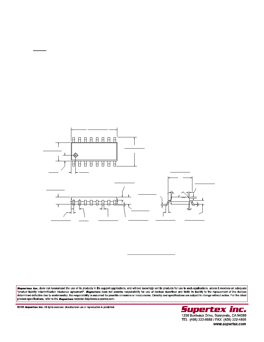
Dimensions in Inches
(Dimensions in Millimeters)
Measurement Legend =
0
∞ - 8 ∞
7
∞ (4 PLCS)
45
∞
7
∞ (4 PLCS)
TYP.
0.500
(12.700)
0.156
± 0.002
(3.962
± 0.051)
0.2335
± 0.0105
(5.931
± 0.267)
TYP.
0.350
(8.890)
0.065
± 0.004
(1.651
± 0.102)
0.020
± 0.002
(0.508
± 0.0508)
TYP.
0.050
(1.270)
0.0165
± 0.0035
(0.4191
± 0.0889)
0.0255
± 0.0005
(0.6475
± 0.0125)
0.006
± 0.002
(0.1524
± 0.0508)
0.059
± 0.002
(1.499
± 0.051)
0.3895
± 0.0045
(9.8935
± 0.1145)
0.193
± 0.012
(4.9022
± 0.3048)
0.013
± 0.004
(0.3302
± 0.1016)
0.033
± 0.017
(0.8382
± 0.4318)
0.009
± 0.002
(0.216
± 0.038)
0.0275
± 0.0025
(0.6985
± 0.0635)
16-LEAD SO PACKAGE (NG) (NARROW BODY)