HV9921/HV9922/HV9923
3-Pin Switch-Mode LED Lamp Driver ICs
1
NR092005
Initial Release
Features
Constant Output Current:
o
HV9921 ≠ 20mA
o
HV9922 ≠ 50mA
o
HV9923 ≠ 30mA
Universal 85-264VAC Operation
Fixed OFF-Time Buck Converter
Internal 500V Power MOSFET
Applications
Decorative Lighting
Low Power Lighting Fixtures
General Description
The HV9921/22/23 are pulse width modulated (PWM)
high-effi ciency LED driver control ICs. They allow effi cient
operation of LED strings from voltage sources ranging up
to 400VDC. The HV9921/22/23 include an internal high
voltage switching MOSFET controlled with fi xed off-time T
OFF
of approximately 10
µs. The LED string is driven at constant
current, thus providing constant light output and enhanced
reliability. The output current is internally fi xed at 20mA for
HV9921, 50mA for HV9922, and 30mA for the HV9923. The
peak current control scheme provides good regulation of the
output current throughout the universal AC line voltage range
of 85 to 264VAC or DC input voltage of 20 to 400V.
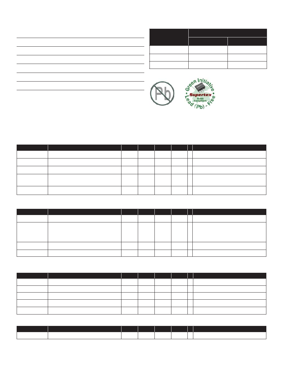
Typical Application Circuit
HV9921/22/23
2
NR092005
HV9921/HV9922/HV9923
Regulator
(V
DD
)
Symbol
Parameter
Min
Typ
Max
Units
Conditions
V
DD
V
DD
Regulator Output
7.1
7.5
7.8
V
V
DRAIN
V
DRAIN
Supply Voltage
20
V
V
UVLO
V
DD
Undervoltage Threshold
5.0
V
V
UVLO
V
DD
Undervoltage Lockout
Hysteresis
200
mV
I
DD
Operating Supply Current
200
350
µ
A
V
DD(EXT)
= 8.5V, V
DRAIN
= 40V
Output (DRAIN)
Symbol
Parameter
Min
Typ
Max
Units
Conditions
V
BR
Breakdown Voltage
500
V
R
ON
ON Resistance ≠ HV9921,22, 23
210
I
DRAIN
= 20mA (HV9921)
I
DRAIN
= 50mA (HV9922)
I
DRAIN
= 30mA (HV9923)
C
DRAIN
Output Capacitance
1
5
pF
V
DRAIN
= 400V
I
SAT
MOSFET Saturation Current
100
150
mA
Current Sense Comparator
Symbol
Parameter
Min
Typ
Max
Units
Conditions
I
TH
Threshold Current ≠ HV9921
20.5
25.5
mA
*
I
TH
Threshold Current ≠ HV9922
52
63
mA
*
I
TH
Threshold Current ≠ HV9923
30.8
38.2
mA
*
T
BLANK
Leading Edge Blanking Delay
200
300
400
ns
*
T
ON(MIN)
Minimum ON Time
650
ns
OFF-Time Generator
Symbol
Parameter
Min
Typ
Max
Units
Conditions
T
OFF
OFF Time
8
10.5
13
µ
s
Ordering Information
DEVICE
Package Options
TO-92
SOT-89
HV9921
HV9921N3-G
HV9921N8-G
HV9922
HV9922N3-G
HV9922N8-G
HV9923
HV9923N3-G
HV9923N8-G
Absolute Maximum Ratings
Supply Voltage, V
DD
-0.3 to +10V
Supply Current, I
DD
+5mA
Operating Ambient Temperature Range
-40∞C to +85∞C
Operating Junction Temperature Range
-40∞ to +125∞C
Storage Temperature Range
-65∞ to +150∞C
Power Dissipation @ 25∞C, TO-92
740mW
Power Dissipation @ 25∞C, SOT-89
1600mW
Mounted on FR4 board, 25mm x 25mm x 1.57mm. Stresses beyond those listed under
"Absolute Maximum Ratings" may cause permanent damage to the device. These are
stress ratings only, and functional operation of the device at these or any other conditions
beyond those indicated in the operational sections of the specifi cations is not implied.
Exposure to absolute maximum rating conditions for extended periods may affect device
reliability.
Electrical Characteristics
(The * denotes the specifi cations which apply over the full operating junction temperature range of
-40
∞
C < T
A
< +85
∞
C, otherwise the specifi cations are at T
A
=25
∞
C, V
DRAIN
=50V, unless otherwise noted)
-G indicates package is RoHS compliant (`Green')

5
NR092005
HV9921/HV9922/HV9923
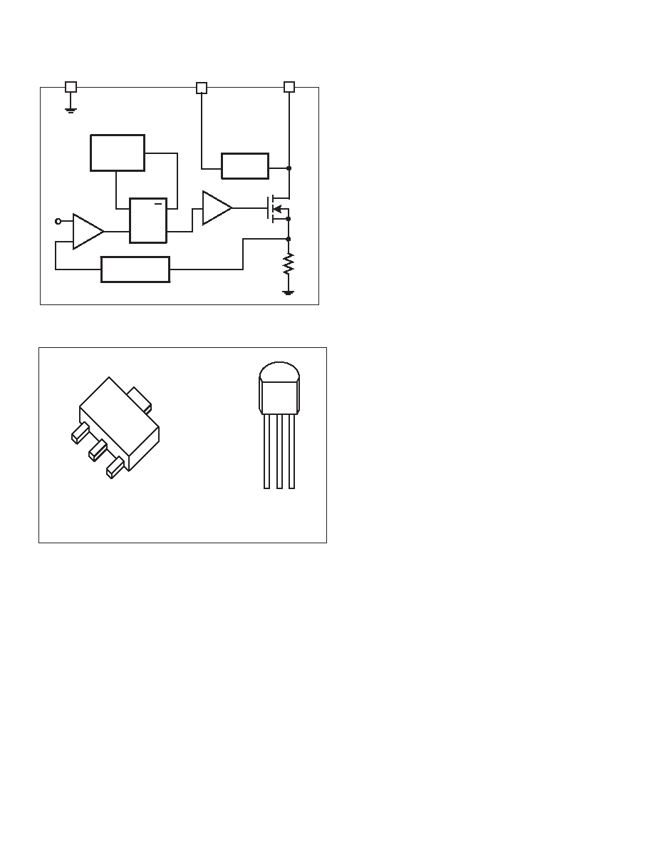
Functional Description
The HV9921/22/23 are PWM peak current controllers
for controlling a buck converter topology in continuous
conduction mode (CCM). The output current is internally
preset at 20mA (HV9921), 50mA (HV9922), or 30mA
(HV9923).
When the input voltage of 20 to 400V appears at the
DRAIN pin, the internal high-voltage linear regulator seeks
to maintain a voltage of 7VDC at the V
DD
pin. Until this
voltage exceeds the internally programmed under-voltage
threshold, the output switching MOSFET is non-conductive.
When the threshold is exceeded, the MOSFET turns on. The
input current begins to fl ow into the DRAIN pin. Hysteresis
is provided in the under-voltage comparator to prevent
oscillation.
When the input current exceeds the internal preset level,
a current sense comparator resets an RS fl ip-fl op, and the
MOSFET turns off. At the same time, a one-shot circuit
is activated that determines the duration of the off-state
(10.5
µS typ.). As soon as this time is over, the fl ip-fl op sets
again. The new switching cycle begins.
A "blanking" delay of 300nS is provided that prevents false
triggering of the current sense comparator due to the leading
edge spike caused by circuit parasitics.
Application Information
The HV9921/22/23 is a low-cost off-line buck converter IC
specifi cally designed for driving multi-LED strings. It can be
operated from either universal AC line range of 85 to 264VAC,
or 20 to 400VDC, and drives up to tens of high brightness
LEDs. All LEDs can be run in series, and the HV9921/22/23
regulates at constant current, yielding uniform illumination.
The HV9921/22/23 is compatible with triac dimmers. The
output current is internally fi xed at 20mA for the HV9921,
50mA for the HV9922, and 30mA for HV9923. These parts
are available in space saving TO-92 and SOT-89 packages.
Selecting L1 and D1
There is a certain trade-off to be considered between
optimal sizing of the output inductor L1 and the tolerated
output current ripple. The required value of L1 is inversely
proportional to the ripple current
I
O
in it.
(1)
V
O
is the forward voltage of the LED string. T
OFF
is the off-
time of the HV9921/22/23. The output current in the LED
string (I
O
) is calculated then as:
(2)
where I
TH
is the current sense comparator threshold.
The ripple current introduces a peak-to-average error in
the output current setting that needs to be accounted for.
Due to the constant off-time control technique used in the
HV9921/22/23, the ripple current is independent of the input
AC or DC line voltage variation. Therefore, the output current
will remain unaffected by the varying input voltage.
Adding a fi lter capacitor across the LED string can reduce
the output current ripple even further, thus permitting a
reduced value of L1. However, one must keep in mind that
the peak-to-average current error is affected by the variation
of T
OFF
. Therefore, the initial output current accuracy might
be sacrifi ced at large ripple current in L1.
Another important aspect of designing an LED driver with the
HV9921/22/23 is related to certain parasitic elements of the
circuit, including distributed coil capacitance of L1, junction
capacitance and reverse recovery of the rectifi er diode D1,
capacitance of the printed circuit board traces C
PCB
and output
capacitance C
DRAIN
of the controller itself. These parasitic
elements affect the effi ciency of the switching converter and
could potentially cause false triggering of the current sense
comparator if not properly managed. Minimizing these
parasitics is essential for effi cient and reliable operation of
the HV9921/22/23.
Coil capacitance of inductors is typically provided in the
manufacturer's data books either directly or in terms of the
self-resonant frequency (SRF).
where L is the inductance value, and C
L
is the coil
capacitance.) Charging and discharging this capacitance
every switching cycle causes high-current spikes in the LED
string. Therefore, connecting a small capacitor C
O
(~10nF) is
recommended to bypass these spikes.
Using an ultra-fast rectifi er diode for D1 is recommended
to achieve high effi ciency and reduce the risk of false
triggering of the current sense comparator. Using diodes
with shorter reverse recovery time t
rr
and lower junction
capacitance C
J
achieves better performance. The reverse
voltage rating V
R
of the diode must be greater than the
maximum input voltage of the LED lamp.
The total parasitic capacitance present at the DRAIN pin of
the HV9921/22/23 can be calculated as:
(3)
When the switching MOSFET turns on, the capacitance C
P
is discharged into the DRAIN pin of the IC. The discharge
current is limited to about 150mA typically. However, it
may become lower at increased junction temperature. The
duration of the leading edge current spike can be estimated
/(
)
L
SRF
1 2
L C
=
P
DRAIN
PCB
L
J
C
C
C
C
C
=
+
+
+
O
OFF
O
V T
L1
I
=
O
TH
O
1
I
I
I
2
=
-