 | –≠–ª–µ–∫—Ç—Ä–æ–Ω–Ω—ã–π –∫–æ–º–ø–æ–Ω–µ–Ω—Ç: HV9930 | –°–∫–∞—á–∞—Ç—å:  PDF PDF  ZIP ZIP |
A090805
1
HV9930
Hysteretic Boost-Buck (Cuk) LED Driver ICs
Features
Constant Output Current
Steps Output Voltage Up or Down
Low EMI
Variable Frequency Operation
Internal 8 to 200V Linear Regulator
Input and output current sensing
Input Current limit
Enable & PWM Dimming
Applications
Automotive LED Drivers
RGB backlight applications
Battery Powered LED Lamps
Other Low Voltage AC/DC or DC/DC LED Drivers
General Description
The HV9930 is a variable frequency PWM controller IC
designed to control an LED lamp driver using a low noise
boost-buck (Cuk) topology. The HV9930 uses hysteretic-
current mode control to regulate both the input and the output
currents. This enables fast transient response (required for
PWM dimming) without the necessity for complex loop
compensation. Input current control enables current limiting
during startup and output overload conditions. Capacitive
isolation protects the LED Lamp from failure of the switching
MOSFET. HV9930 provides a low-frequency PWM dimming
input that can accept an external control signal with a duty ratio
of 0-100%.
The HV9930 based LED driver is ideal for automotive LED
lamps and RGB backlight applications with low voltage DC
inputs. The HV9930 based LED Lamp drivers can achieve
efficiency in excess of 80%.
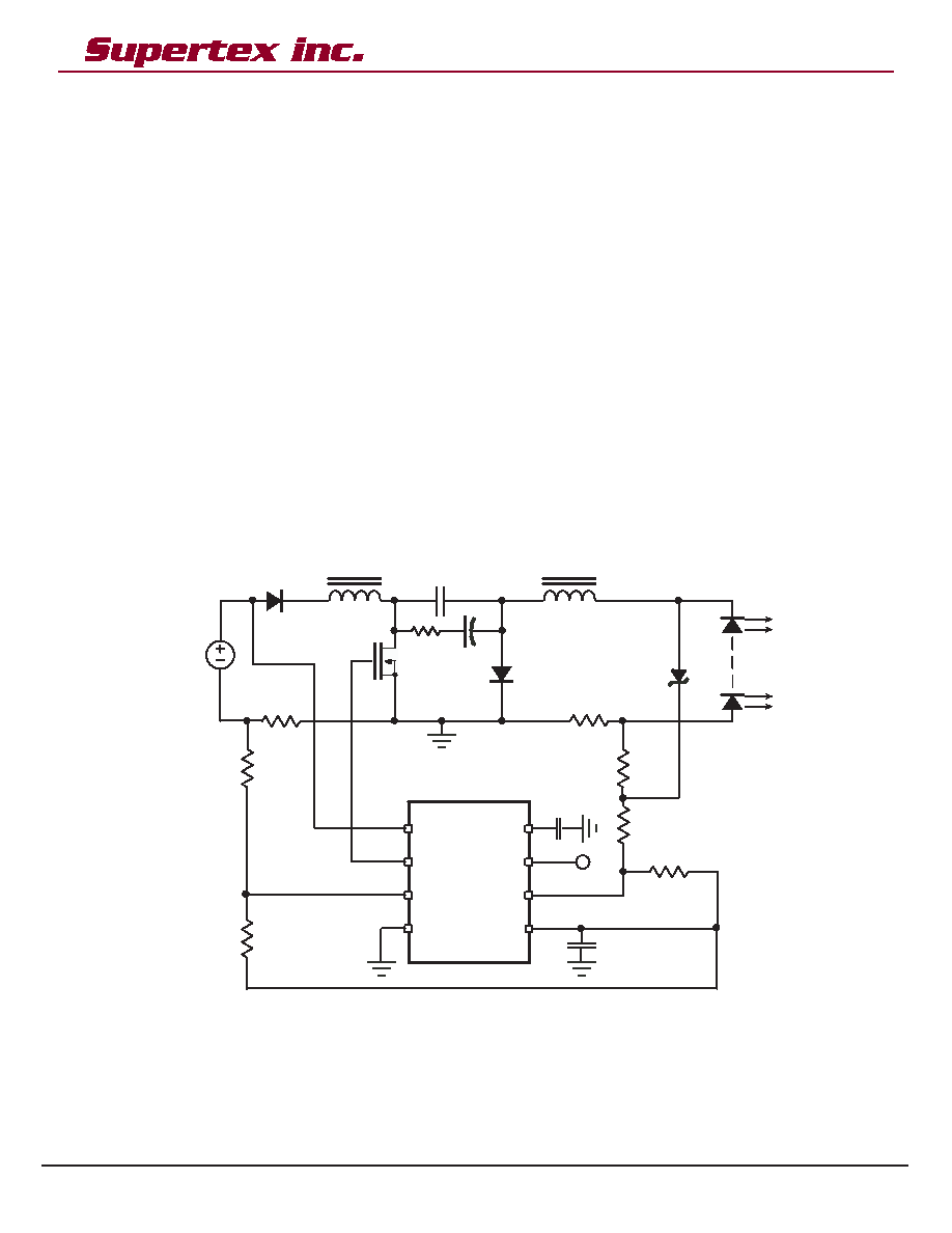
Typical Application Circuit
HV9930
V
IN
GATE
CS1
CS2
V
DD
PWMD
REF
GND
HV9930
VDC
L1
L2
C1
Q1
D1
Rcs1
Rcs2
Rref2
Rref1
Rs1
Rs2b
C2
D2
VO
+
-
C3
Rs2a
D3
Rd
Cd
Supertex inc.
∑
1235 Bordeaux Drive, Sunnyvale, CA 94089
∑
Tel: (408) 222-8888
∑
FAX: (408) 222-4895
∑
www.supertex.com
A090805
A090805
2
HV9930
Ordering Information
Package Options
Device
8 pin SOIC
8 pin DIP
HV9930 HV9930LG-G
HV9930P-G
-G indicates package is RoHS compliant `Green'
Absolute Maximum Ratings
V
IN
to GND..................................... -0.5V to +200V
V
DD
to GND...................................
-0.3V to +13.5V
CS1, CS2 to GND............................. -0.3V to V
DD
+ 0.3V
PWMD to GND................................. -0.3V to (V
DD
+ 0.3V)
GATE to GND................................... 0.3V to (V
DD
+ 0.3V)
Continuous Power Dissipation (TA = +25∞C) (Note 1)
8-Pin DIP (derate 9mW/∞C above +25∞C)............ 900mW
8-Pin SO (derate 6.3mW/∞C above 25∞C)........... 630mW
Operating Temperature Range ...................-40∞C to +85∞C
Junction Temperature..................................+125∞C
Storage Temperature Range .......................-65∞C to +150∞C
Stresses beyond those listed under ``Absolute Maximum Ratings'' may cause
permanent damage to the device. These are stress ratings only, and
functional operation of the device at these or any other conditions beyond
those indicated in the operational sections of the specifications is not
implied. Exposure to absolute maximum rating conditions for extended
periods may affect device reliability.
Electrical Characteristics
(The * denotes the specifications which apply over the full operating junction temperature range of 0
∞
C < T
A
< +85
∞
C, otherwise the specifications are
at T
A
= 25
∞
C, V
DD
= 7.5V, unless otherwise noted)
Symbol Description Min
Typ
Max Units
Conditions
Input
V
INDC
Input DC supply voltage range*
8
200
V
DC input voltage
I
INsd
Shut-Down mode supply current*
0.5
1
mA
PWM_D connected to GND,
V
IN
= 12V
Internal Regulator
V
DD
Internally regulated voltage
7.0
7.5
9.0
V
V
IN
= 8≠200V, I
DD(ext)
= 0,
GATE open
I
DD(ext)
V
DD
current available for external
circuitry
1
1.0
mA
V
IN
= 8≠200V
UVLO
V
DD
under voltage lockout
threshold
6.45 6.7 6.95 V
V
IN
rising
UVLO
V
DD
under voltage lockout
hysteresis
500 mV
V
DD(ext)
Steady State external voltage
which can applied at the V
DD
pin
12
V
Reference
V
REF
REF pin voltage*
1.212
1.25
1.288
V
REF bypassed with a 0.1
µF capacitor
to GND; I
REF
= 0;
V
DD
= 7.5V; PWMD = 5V
V
REFLINE
Line regulation of reference voltage
0
20
mV
REF bypassed with a 0.1
µF capacitor
to GND; I
REF
= 0;
V
DD
= 7 ≠ 12V; PWMD = 5V
I
REF
Reference Output current range
1
-0.01 1.0
mA
REF bypassed with a 0.1
µF capacitor
to GND; V
DD
= 7 ≠ 12V; PWMD = 5V
V
REFLOAD
Load regulation of reference
voltage
0
25
mV
REF bypassed with a 0.1
µF capacitor
to GND; I
REF
= 0 ≠ 500µA;
V
DD
= 7.5; PWMD = 5V
PWM Dimming
V
PWMD(lo)
PWMD input low voltage*
0.8
V
V
IN
= 10 - 200V
V
PWMD(hi)
PWMD input high voltage*
2.4
V
V
IN
= 10 - 200V
R
PWMD
PWMD pull-down resistance
50
100
150
k
V
PWMD
= 5V
A090805
3
HV9930
Gate
I
SOURCE
GATE short circuit current, sourcing
0.165
A
V
GATE
= 0V; V
DD
= 7.5V
I
SINK
GATE
sinking
current
0.165
A V
GATE
= 10V ; V
DD
= 7.5V
T
RISE
GATE output rise time
30
50
ns
C
GATE
= 500pF; V
DD
= 7.5V
T
FALL
GATE output fall time
30
50
ns
C
GATE
= 500pF; V
DD
= 7.5 V
Input Current Sense Comparator
V
TURNON1
Voltage required to turn GATE on
*
88 100
112
mV
CS2 = 200mV ; CS1 increasing ;
GATE goes LOW to HIGH
V
TURNOFF1
Voltage required to turn GATE off
*
-12 0 12
mV
CS2 = 200mV ; CS1 decreasing ;
GATE goes HIGH to LOW
T
D1, ON
Delay to Output (turn-on)
150
250
ns
CS2=200mV ;
CS1 = 50mV to 200mV step
T
D1, OFF
Delay to Output (turn-on)
150
250
ns
CS2=200mV ;
CS1 = 50mV to ≠100mV step
Output Current Sense Comparator
V
TURNON2
Voltage required to turn GATE on
*
88 100
112
mV
CS1 = 200mV ; CS2 increasing ;
GATE goes LOW to HIGH
V
TURNOFF2
Voltage required to turn GATE off
*
-12 0 12
mV
CS1 = 200mV ; CS2 decreasing ;
GATE goes HIGH to LOW
T
D2, ON
Delay to Output (turn-on)
150
250
ns
CS1=200mV ;
CS2 = 50mV to 200mV step
T
D2, OFF
Delay to Output (turn-on)
150
250
ns
CS1=200mV ;
CS2 = 50mV to ≠100mV step
1
Also limited by package power dissipation limit, whichever is lower.
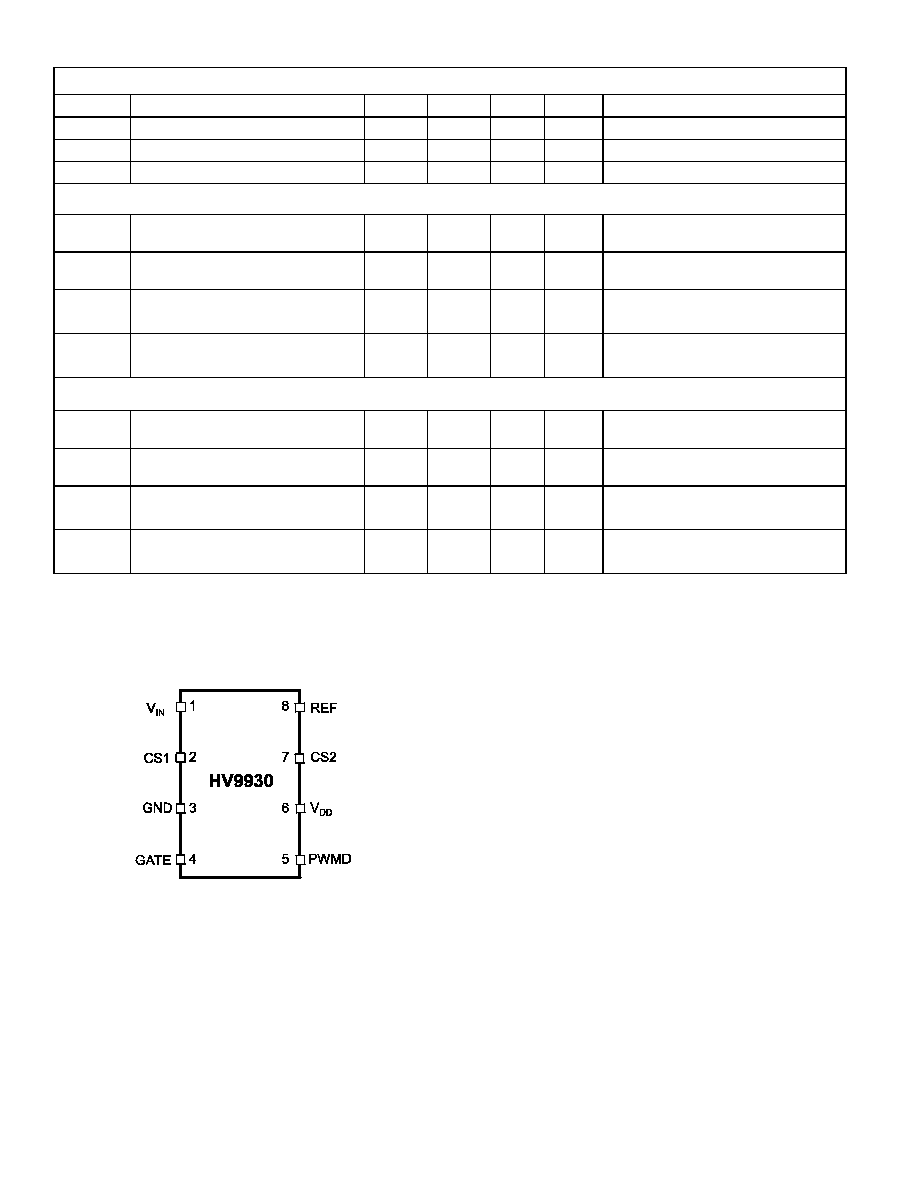
Pinout
Pin Description
V
IN
≠ This pin is the input of a 8-200V voltage regulator.
V
DD
≠ This is a power supply pin for all internal circuits. It
must be bypassed with a low ESR capacitor to GND.
GATE ≠ This pin is the output gate driver for an external N-
channel power MOSFET.
GND ≠ Ground return for all the internal circuitry. This pin
must be electrically connected to the ground of the power
train.
REF ≠ This pin provides accurate reference voltage. It must
be bypassed with a 0.01-0.1uF capacitor to GND.
PWM ≠ When this pin is pulled to GND, switching of the
HV9930 is disabled. When the PWM pin is released, or
external TTL high level is applied to it, switching will
resume. This feature is provided for applications that require
PWM dimming of the LED lamp.
CS1 and CS2 ≠ These pins are used to sense the input and
output currents of the boost-buck converter. They are the
non-inverting inputs of the internal comparators.

A090805
4
HV9930
Functional Block Diagram
Regulator
100mV
7.5V
V
IN
CS1
CS2
PWMD
GATE
V
DD
REF
GND
1.25V
HV9930
Input
Comparator
Output
Comparator

A090805
5
HV9930
Functional Description
Power Topology
The HV9930 is optimized to drive a continuous conduction
mode (CCM) boost-buck DC/DC converter topology commonly
referred to as "Cuk converter" (see Circuit Diagram on page 1).
This power converter topology offers numerous advantages
useful for driving high-brightness light emitting diodes (HB
LED). These advantages include step-up or step-down voltage
conversion ratio and low input and output current ripple. The
input and the output inductors can also share a common core.
The output load is decoupled from the input voltage with a
capacitor making the driver inherently failure-safe for the
output load.
The HV9930 offers a simple and effective control technique for
use with a boost-buck LED driver. It uses two hysteretic mode
controllers ≠ one for the input and one for the output. The
outputs of these two hysteretic comparators are AND together,
and used to drive the external FET. This control scheme gives
accurate current control and constant output current in the
presence of input voltage transients without the need for
complicated loop design.
Input Voltage Regulator
The HV9930 can be powered directly from its V
IN
pin that takes
a voltage from 8V to 200V. When a voltage is applied at the
V
IN
pin, the HV9930 tries to maintain a constant 7.5V (typ) at
the V
DD
pin. The regulator also has a built in under-voltage
lockout which shuts off the IC if the voltage at the V
DD
pin falls
below the UVLO threshold.
The V
DD
pin must be bypassed by a low ESR capacitor
(
0.1µF) to provide a low impedance path for the high
frequency current of the output gate driver.
The IC can also be operated by supplying a voltage at the V
DD
pin greater than the internally regulated voltage. This will turn
off the internal linear regulator and the IC will function by
drawing power from the external voltage source connected to
the V
DD
pin.
In case of input transients that reduce the input voltage below
8V (like cold crank condition in an automotive system), the V
IN
pin of the HV9930 can be connected to the drain of the
MOSFET through a diode. Since the drain of the FET is at a
voltage equal to the sum of the input and output voltages, the
IC will still be operational when the input goes below 8V. In
these cases, a larger capacitor is needed to the V
DD
pin to
supply power to the IC when the MOSFET is ON.
Reference
An internally trimmed voltage reference of 1.25V (+/- 3%) is
provided at the REF pin. The reference can supply a
maximum output current of 1mA to drive external circuitry.
This reference can be used to set the current thresholds of the
two comparators as shown in the Typical Application Circuit.
Current Comparators
The HV9930 features two identical comparators with a built-in
100mV hysteresis. When the GATE is low, the inverting
terminal is connected to 100mV and when the GATE is high, it
is connected to GND. One comparator is used for the input
current control and the other for the output current control.
The input side hysteretic controller is in operation only during
start-up and overload conditions. This ensures that the input
current never exceeds the designed value. During normal
operation, the input current will be less than the programmed
current and hence, the output of the input side comparator will
be HIGH. The output of the AND gate will then be dictated by
the output current controller.
The output side hysteretic comparator will be in operation
during the steady state operation of the circuit. This
comparator turns the MOSFET on and off based on the LED
current.
The use of these comparators in a boost-buck topology is a
patent-pending technique, which eliminates the need for
compensation components.
PWM Dimming
PWM Dimming can be achieved by applying a TTL-compatible
square wave signal at the PWM pin. When the PWMD pin is
pulled high, the gate driver is enabled and the circuit operates
normally. When the PWMD pin is left open or connected to
GND, the gate driver is disabled and the external MOSFET
turns off. The IC is designed so that the signal at the PWMD
pin inhibits the driver only and the IC need not go through the
entire start-up cycle each time ensuring a quick response time
for the output current.
The flying capacitor in the Cuk converter (C1) is initially
charged to the input Voltage VDC (through diodes D1 and D2).
When the circuit is turned on and reaches steady state, the
voltage across C1 will be VDC+VO. In the absence of diode
D2, when the circuit is turned off, capacitor C1 will discharge
through the LEDs and the input voltage source VDC. Thus,
during PWM dimming, if capacitor C1 has to charged and
discharged each cycle, the transient response of the circuit will
be limited. By adding diode D2, the voltage across capacitor
C1 is held at VDC+VO even when the circuit is turned off
enabling the circuit to return quickly to its steady state (and
bypassing the start-up stage) upon being enabled.
Application Information
Over-voltage Protection
Over-voltage protection can be added by splitting the output
side resistor Rs2 into two components and adding a zener
diode D3. When there is an open LED condition, the diode D3
will clamp the output voltage and the zener diode current will
be regulated by the sum of Rs2a and Rcs2.
Damping Circuit
The Cuk converter is inherently unstable when the output
current is being controlled. An uncontrolled input current will
lead to an un-damped oscillation between L1 and C1 causing
excessively high voltages across C1. To prevent these
oscillations, a damping circuit consisting of Rd and Cd is
applied across the capacitor C1. This damping circuit will help
to stabilize the circuit and help in the proper operation of the
HV9930 based Cuk converter.
Design and Operation of the Boost-Buck Converter
For details on the design for a Boost-Buck converter using the
HV9930 and the calculation of the damping components,
please refer to Application Note AN-H51.

A090805
6
HV9930
Design Example
The choice of the resistor dividers to set the input and output
current levels is illustrated by means of the design example
given below.
The parameters of the power circuit are:
kHz
300
f
A
35
.
0
I
V
28
V
V
16
V
V
9
V
min
s
o
o
max
in
min
in
=
=
=
=
=
Using these parameters, the values of the power stage
inductors and capacitor can be computed as (see Application
Note AN-H51 for details):
F
22
.
0
1
C
H
150
2
L
H
82
1
L
µ
µ
µ
=
=
=
The input and output currents for this design are:
mA
5
.
87
I
mA
350
I
A
21
.
0
I
A
6
.
1
I
o
o
in
max
in
=
=
=
=
Output Current Limits
The current sense resistor (
2
cs
R
), combined with the other
resistors (
2
ref
2
s
R
&
R
), determines the output current limits.
The current sense resistor (
1
cs
R
), combined with the other
resistors (
1
ref
1
s
R
&
R
), determines the input current limits.
The resistors can be chosen using the following equations:
V
05
.
0
R
R
V
2
.
1
R
I
f
Re
s
cs
-
◊
=
◊
(1)
V
1
.
0
R
R
V
1
.
0
R
I
f
Re
s
cs
+
◊
=
◊
(2)
Where
I
is the current (either
o
I
or
in
I
) and
I
is the peak-to-
peak ripple in the current (either
o
I
or
in
I
).
For the input side, the current level used in the equations
should be larger than the maximum input current so that it
does not interfere with the normal operation of the circuit. The
peak input current can be computed as:
A
706
.
1
2
I
I
I
in
max
,
in
pk
,
in
=
+
=
(3)
Assuming a 30% peak-to-peak ripple when the converter is in
input current limit mode, the minimum value of the input current
will be:
lim
,
in
min
lim,
I
85
.
0
I
=
.
(4)
Setting
pk
,
in
min
lim,
I
05
.
1
I
=
,
(5)
The current level to limit the converter can then be computed.
A
1
.
2
I
85
.
0
05
.
1
I
inpk
lim
in
=
=
(6)
Using
A
35
.
0
I
o
=
and
A
0875
.
0
I
o
=
in (1) and (2),
5625
.
0
R
R
78
.
1
R
2
ref
2
s
2
cs
=
=
Before the design of the output side is complete, over voltage
protection has to be included in the design. For this
application, choose a 33V zener diode. This is the voltage at
which the output will clamp in case of an open LED condition.
For a 350mW diode, the maximum current rating at 33V works
out to about 10mA. Using a 2.5mA current level during open
LED conditions, and assuming the same
2
ref
2
s
R
R
ratio,
120
R
R
a
2
s
2
cs
=
+
.
(6)
Choose the following values for the resistors:
%
1
,
W
4
/
1
,
65
.
1
R
2
cs
=
%
1
,
W
8
/
1
,
k
10
R
2
ref
=
%
1
,
W
8
/
1
,
100
R
a
2
s
=
%
1
,
W
8
/
1
,
k
23
.
5
R
b
2
s
=
The current sense resistor needs to be at least a 1/4W, 1%
resistor.
Similarly, using
A
1
.
2
I
in
=
and
A
63
.
0
I
3
.
0
I
in
in
=
◊
=
in
(1) and (2),
442
.
0
R
R
1
ref
1
s
=
W
1
R
I
P
228
.
0
R
1
cs
2
lim
,
in
1
Rcs
1
cs
=
=
=
Choose the following values for the resistors:
resistors
%
5
,
W
2
/
1
,
68
.
0
three
of
n
combinatio
parallel
R
1
cs
=
%
1
,
W
8
/
1
,
k
10
R
1
ref
=
%
1
,
W
8
/
1
,
k
42
.
4
R
1
s
=
A090805
7
HV9930
DSFP-HV9930
A090805
Note: Circle (e.g. B ) indicates JEDEC Reference.
Dimensions in Inches
(Dimensions in Millimeters)
Measurement Legend =
0.395 max
0.030 -
0.110
0.300 - 0.320
0.020
0.009 - 0.015
+0.025
-0.015
0.325
0.250
± 0.005
0.250
± 0.015
0.040
(1.016) TYP
0.125 min.
0.130
± 0.005
0.020 min.
0.018
± 0.003
0.100
± 0.010
0
∞ - 10∞!
1
8-LEAD PLASTIC DUAL IN-LINE PACKAGE (P)
D
H
1
E
H
A
A
1
e
B
C
L
h
0.020
± 0.009
(0.508
± 0.2286)
L
1
0.0275
± 0.0025
(0.6985
± 0.0635)
Note: Circle (e.g. B ) indicates JEDEC Reference.
Dimensions in Inches
(Dimensions in Millimeters)
Measurement Legend =
8-LEAD SMALL OUTLINE PACKAGE (LG) (MS-012AA)