 | –≠–ª–µ–∫—Ç—Ä–æ–Ω–Ω—ã–π –∫–æ–º–ø–æ–Ω–µ–Ω—Ç: HV9931 | –°–∫–∞—á–∞—Ç—å:  PDF PDF  ZIP ZIP |
HV9931
HV9931 Unity Power Factor LED Lamp Driver
1
NR081505
Initial Release
Features
Constant Output Current
Large Step-Down Ratio
Unity Power Factor
Low Input Current Harmonic Distortion
Fixed Frequency or Fixed Off-Time Operation
Internal 450V Linear Regulator
Input and output current sensing
Input Current limit
Enable, PWM and Phase Dimming
Applications
Offl ine LED Lamps and Fixtures
Street lamps
Traffi c Signals
Decorative Lighting
General Description
The HV9931 is a fi xed frequency PWM controller IC designed
to control an LED lamp driver using a single-stage PFC
buckboost-buck topology. It can achieve a unity power factor
and a very high step-down ratio that enables driving a single
high-brightness LED from the 85-264VAC input without a
need for a power transformer. This topology allows reducing
the fi lter capacitors and using non-electrolytic capacitors to
improve reliability. The HV9931 uses open-loop peak current
control to regulate both the input and the output current. This
control technique eliminates a need for loop compensation,
limits the input inrush current, and is inherently protected
from input under-voltage condition. Capacitive isolation
protects the LED Lamp from failure of the switching MOSFET.
HV9931 provides a low-frequency PWM dimming input that
can accept an external control signal with a duty ratio of 0-
100% and a frequency of up to a few kilohertz. The PWM
dimming capability enables HV9931 phase control solutions
that can work with standard wall dimmers.
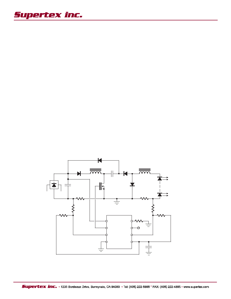
Typical Application Circuit
V
IN
GATE
CS1
CS2
V
DD
PWMD
RT
GND
R
ref2
R
ref1
R
CS1
R
CS2
C2
V
IN
L1
L2
C1
Q1
D3
R
S1
R
S2
D4
VO
+
-
D1
D2
~AC
~AC
C
IN
RT
HV9931
2
NR081505
HV9931
Ordering Information
DEVICE
Package Options
8-Lead SOIC
8-Lead DIP
HV9931
HV9931LG-G
HV9931P-G
-G indicates package is RoHS compliant (`Green')
Absolute Maximum Ratings
V
IN
to GND
-0.5V to +470V
V
DD
to GND
-0.3V to +13.5V
CS1, CS2 to GND
-0.3V to V
DD
+ 0.3V
PWMD to GND
-0.3V to (V
DD
+ 0.3V)
GATE to GND
-0.3V to (V
DD
+ 0.3V)
Continuous Power Dissipation (TA = +25∞C)
-
Also limited by package power dissipation limit, whichever is lower.
8-Pin DIP (derate 9mW/∞C above +25∞C)
900mW
8-Pin and 14-Pin SO (derate 6.3mW/∞C above +25∞C)
630mW
Operating Temperature Range
-40∞C to +85∞C
Junction Temperature
+125∞C
Storage Temperature Range
-65∞C to +150∞C
Symbol
Parameter
Min
Typ
Max
Units
Conditions
Input
V
INDC
Input DC supply voltage range*
8
450
V
DC input voltage
I
INSD
Shut-Down mode supply current*
0.5
1
mA
PWMD connected to GND, V
IN
= 12V
Internal Regulator
V
DD
Internally regulated voltage*
7.12
7.5
7.88
V
V
IN
= 8≠450V, I
DD(ext)
= 0, GATE open
UVLO
V
DD
undervoltage lockout threshold
6.45
6.7
6.95
V
V
IN
rising
UVLO
V
DD
undervoltage lockout hysteresis
500
mV
PWM Dimming
V
PWMD(lo)
PWMD input low voltage*
1.0
V
V
IN
= 8≠450V
V
PWMD(hi)
PWMD input high voltage*
2.4
V
V
IN
= 8≠450V
R
PWMD
PWMD pull-down resistance
50
100
150
k
V
PWMD
= 5V
GATE
V
GATE(hi)
GATE high output voltage*
V
DD
-0.3
V
DD
V
I
GATE
= 10mA
V
GATE(lo)
GATE low output voltage*
0
0.3
V
I
GATE
= -10mA
T
RISE
GATE output rise time
30
50
ns
C
GATE
= 500pF
T
FALL
GATE output fall time
30
50
ns
C
GATE
= 500pF
T
DELAY
Delay from CS trip to GATE
150
300
ns
V
IN
= 12V, V
CSI,
V
CS2
= -50mV
T
BLANK
Blanking delay
150
215
280
ns
V
CSI,
V
CS2
= -0.15V
Electrical Characteristics
(The * denotes the specifi cations which apply over the full operating junction temperature range of -40∞C < T
A
< +85∞C, otherwise the specifi cations are at
T
A
= 25∞C, V
IN
= 100V, unless otherwise noted)
Stresses beyond those listed under "Absolute Maximum Ratings" may cause permanent damage to the device. These are stress ratings only, and functional operation of the
device at these or any other conditions beyond those indicated in the operational sections of the specifi cations is not implied. Exposure to absolute maximum rating conditions
for extended periods may affect device reliability.
3
NR081505
HV9931
Symbol
Parameter
Min
Typ
Max
Units
Conditions
Oscillator
F
OSC
Initial Accuracy
80
100
120
kHz
RT = 230K
F
T
Temperature Stability
3
%
Tj = -40∞C to +125∞C
Comparators
V
OFFSET1
V
OFFSET2
Comparator Input offset voltage
*
-12
12
mV
V
OFFSET1
V
OFFSET2
Input offset voltage temperature drift
10
µV/∞C
Tj = -40∞C to +125∞C
V
IN
≠ This pin is the input of a high voltage regulator.
V
DD
≠ This is a power supply pin for all internal circuits. It must be bypassed with a low
ESR capacitor to GND.
GATE ≠ This pin is the output gate driver for an external N-channel power MOSFET.
GND ≠ Ground return for all the internal circuitry. This pin must be electrically connected
to the ground of the power train.
RT ≠ Oscillator control. A resistor connected between this pin and GND sets the PWM
frequency. A resistor connected between this pin and GATE sets the PWM off-time.
PWMD ≠ When this pin is pulled to GND, switching of the HV9931 is disabled. When the
PWMD pin is released, or external TTL high level is applied to it, switching will resume.
This feature is provided for applications that require PWM dimming of the LED lamp.
CS1 and CS2 ≠ These pins are used to sense the input and output currents of the
converter. They are the inverting inputs of the internal comparators.
Pin Description
V
IN
GATE
CS1
RT
GND
V
DD
PWMD
CS2
1
2
3
4
8
7
6
5
HV9931
SOIC-8, DIP-8
Pinout
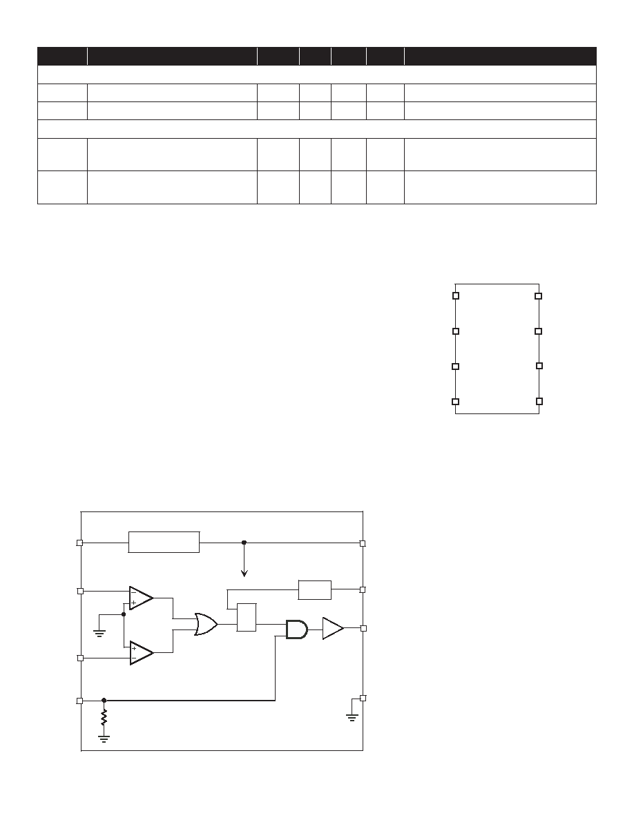
Functional Block Diagram
REGULATOR
7.5V
V
IN
CS
1
CS2
PWMD
GATE
V
DD
RT
R Q
S
OSC
AGND
HV9931
4
NR081505
HV9931
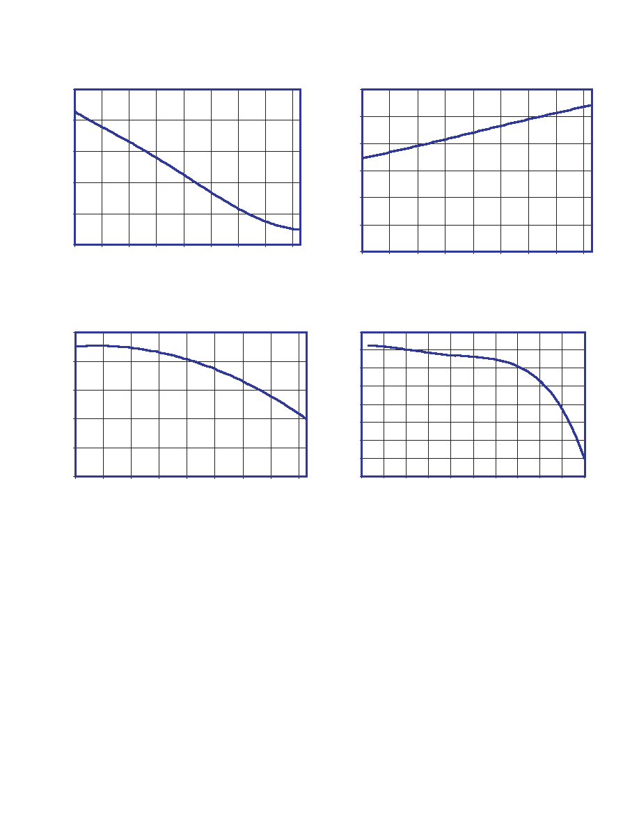
Typical Performance Characteristics
(T
J
= 25
O
C, V
IN
=100V unless otherwise noted)
7.45
7.5
7.55
7.6
7.65
7.7
-40
-20
0
20
40
60
80
100
120
Junction Tem perature (∞C)
V
DD
(V
)
0
50
100
150
200
250
300
-40
-20
0
20
40
60
80
100
120
Junction Tem perature (∞C)
T
BLANK
(n
s
)
4
4.5
5
5.5
6
6.5
7
7.5
8
0
2
4
6
8
10
12
14
16
18
20
I
IN
(mA)
V
DD
(V)
88
89
90
91
92
93
-40
-20
0
20
40
60
80
100
120
Junction Tem perature (∞C)
Fr
e
que
nc
y
(
k
H
z
)
V
DD
vs. Junction Temperature (L
IN
= 2mA)
Blanking Delay vs. Junction Temperature
Frequency vs. Junction Temperature (RT = 226K)
V
DD
vs. Regulator Current (V
IN
= 100V)

5
NR081505
HV9931
Functional Description
Power Topology
The HV9931 is optimized to drive Supertex's proprietary single-
stage, single-switch, non-isolated topology, cascading an input
power factor correction (PFC) buck-boost stage and an output
buck converter power stage. This power converter topology offers
numerous advantages useful for driving high-brightness light
emitting diodes (HB LED). These advantages include unity power
factor, low harmonic distortion of the input AC line current, and low
output current ripple. The output load is decoupled from the input
voltage with a capacitor making the driver inherently failure-safe for
the output load. The power converter topology also permits reducing
the size of a fi lter capacitor needed, enabling use of non-electrolytic
capacitors. The latter advantage greatly improves reliability of the
overall solution.
The HV9931 is a peak current-mode controller that is specifi cally
designed to drive a constant current buckboost-buck power
converter. This patent pending control scheme features two identical
current sense comparators for detecting negative current signal
levels. One of the comparators regulates the output LED current.
The other one is used for sensing the input inductor current. The
second comparator is mainly responsible for the converter start-
up. The control scheme inherently features low inrush current
and input under-voltage protection. The HV9931 can operate with
programmable constant frequency or constant off-time. In many
cases, the constant off-time operating mode is preferred, since
it improves line regulation of the output current, reduces voltage
stress of the power components and simplifi es regulatory EMI
compliance. (See Application Note AN-H52.)
Input Voltage Regulator
The HV9931 can be powered directly from its V
IN
pin and takes a
voltage from 8V to 450V. When a voltage is applied at the V
IN
pin,
the HV9931 seeks to maintain a constant 7.5V at the V
DD
pin. The
V
DD
voltage can be also used as a reference for the current sense
comparators. The regulator is equipped with an under-voltage
protection circuit which shuts off the HV9931 when the voltage at
the V
DD
pin falls below 6.2V.
The V
DD
pin must be bypassed by a low ESR capacitor ( 0.1µF) to
provide a low impedance path for the high frequency current of the
output gate driver.
The HV9931 can also be operated by supplying a voltage at the V
DD
pin greater than the internally regulated voltage. This will turn off
the internal linear regulator and the HV9931 will function by drawing
power from the external voltage source connected to the V
DD
pin.
PWM Dimming and Wall Dimmer Compatibility
PWM Dimming can be achieved by applying a TTL-compatible
square wave signal at the PWMD pin. When the PWMD pin is
pulled high, the gate driver is enabled and the circuit operates
normally. When the PWMD pin is left open or connected to GND,
the gate driver is disabled and the external MOSFET turns off. The
HV9931 is designed so that the signal at the PWMD pin inhibits the
driver only, and the IC need not go through the entire start-up cycle
each time ensuring a quick response time for the output current.
The power topology requires little fi lter capacitance at the output,
since the output current of the buck stage is continuous, and since
AC line fi ltering is accomplished through the middle capacitor rather
than the output one. Therefore, disabling the HV9931 via its PWMD
or V
IN
pins can interrupt the output LED current in accordance with
the phase-controlled voltage waveform of a standard wall dimmer.
Oscillator
Connecting an external resistor from RT pin to GND programs
switching frequency:
Connecting the resistor from RT pin to GATE programs constant
off-time:
Input and Output Current Feedback
Two current sense comparators are included in the HV9931. Both
comparators have their non-inverting inputs internally connected to
ground (GND). The CS1 and CS2 inputs are inverting inputs of the
comparators. Connecting a resistor divider into either of these inputs
from a positive reference voltage and a negative current sense
signal programs the current sense threshold of the comparator. The
V
DD
voltage of the HV9931 can be used as the reference voltage.
(If more accuracy is needed, an external reference voltage can be
applied.) When either the CS
1
or the CS
2
pin voltage falls below
GND, the GATE pulse is terminated. A leading edge blanking delay
of 215ns (typ) is added. The GATE voltage becomes high again
upon receiving the next clock pulse of the oscillator circuit.
Referring to the Functional Circuit Diagram, the CS2 comparator is
responsible for regulating output current. The output LED current
can be programmed using the following equation:
where I
L2
is the peak-to-peak current ripple in L2. The CS1
comparator limits the current in the input inductor L1. There is
no charge in the capacitor C1 upon the start-up of the converter.
Therefore, L2 cannot develop the output current, and the HV9931
starts-up in the input current limiting mode. The CS1 current
threshold must be programmed such that no input current limiting
occurs in normal steady-state operation. The CS1 threshold can be
programmed in accordance with a similar equation:
where I
L1(PK)
is the maximum peak current in L1.
MOSFET Gate Driver
Typically, the gate driving capability of the HV9931 is limited by the
amount of power dissipation in its linear regulator. Thus, care must
be taken selecting a switching MOSFET to be used in the circuit.
An optimal trade-off must be found between the gate charge and
the on-resistance of the MOSFET to minimize the input regulator
current.
[ ]
[ ]
S
T
25000
F kHz
R K
22
=
+
[ ]
[ ]
T
OFF
R K
22
T
s
25
µ
+
=
.
L2
CS 2
REF 2
S 2
1
Io
I
2
R
R
R
7 5V
+
=
(
)
.
L1 PK
CS1
REF 1
S1
I
R
R
R
7 5V
=
6
NR081505
HV9931
Functional Circuit Diagram
V
IN
L1
L2
C1
Q1
D3
R
S1
R
S2
R
ref2
Rref1
R
CS1
R
CS2
D4
VO
+
-
7. 5V
V
S1
+
_
V
S2
+
_
V
C1
+
_
i
L2
i
L1
Q
R
S
D1
D2
~AC
~AC
C
IN
OSC
RE G
C
DD
GND
PWMD
CS2
V
IN
CS1
RT
GATE
V
DD
RT
HV9931
i
L2
i
L1
V
DD
0
0
0
t
t
t
GATE
Switching Waveform
7
Doc.# DSFP - HV9931 NR081505
HV9931
Note: Circle (e.g. B ) indicates JEDEC Reference.
Dimensions in Inches
(Dimensions in Millimeters)
Measurement Legend =
0.395 max
0.030 -
0.110
0.300 - 0.320
0.020
0.009 - 0.015
+0.025
-0.015
0.325
0.250
± 0.005
0.250
± 0.015
0.040
(1.016) TYP
0.125 min.
0.130
± 0.005
0.020 min.
0.018
± 0.003
0.100
± 0.010
0
∞ - 10∞
1
8-Lead Plastic Dual In-Line Package (P)
0
∞ - 8 ∞
45
∞
7
∞ (4 PLCS)
0.193
± 0.012
(4.9022
± 0.3048)
D
0.192
± 0.005
(4.8895
± 0.1143)
H
1
0.154
± 0.004
(3.9116
± 0.1016)
E
0.236
± 0.008
(5.9944
± 0.2032)
H
0.061
± 0.008
(1.5494
± 0.2032)
A
0.007
± 0.003
(0.1778
± 0.0762)
A
1
TYP.
0.050
(1.270)
e
0.016
± 0.002
(0.4064
± 0.0508)
B
C
0.010
± 0.002
(0.254
± 0.0508)
0.035
± 0.015
(0.889
± 0.381)
L
h
0.020
± 0.009
(0.508
± 0.2286)
L
1
0.0275
± 0.0025
(0.6985
± 0.0635)
8-Lead Small Outline Package (LG)