 | –≠–ª–µ–∫—Ç—Ä–æ–Ω–Ω—ã–π –∫–æ–º–ø–æ–Ω–µ–Ω—Ç: LND150ND | –°–∫–∞—á–∞—Ç—å:  PDF PDF  ZIP ZIP |

1
12/13/01
Supertex Inc. does not recommend the use of its products in life support applications and will not knowingly sell its products for use in such applications unless it receives an adequate "products liability
indemnification insurance agreement." Supertex does not assume responsibility for use of devices described and limits its liability to the replacement of devices determined to be defective due to
workmanship. No responsibility is assumed for possible omissions or inaccuracies. Circuitry and specifications are subject to change without notice. For the latest product specifications, refer to the
Supertex website: http://www.supertex.com. For complete liability information on all Supertex products, refer to the most current databook or to the Legal/Disclaimer page on the Supertex website.
Absolute Maximum Ratings
Drain-to-Source Voltage
BV
DSX
Drain-to-Gate Voltage
BV
DGX
Gate-to-Source Voltage
±20V
Operating and Storage Temperature
-55∞C to +150∞C
Soldering Temperature*
300∞C
*
Distance of 1.6 mm from case for 10 seconds.
LND150
Advanced DMOS Technology
The LND1 is a high voltage N-channel depletion mode (normally-
on) transistor utilizing Supertex's lateral DMOS technology. The
gate is ESD protected.
The LND1 is ideal for high voltage applications in the areas of
normally-on switches, precision constant current sources, volt-
age ramp generation and amplification.
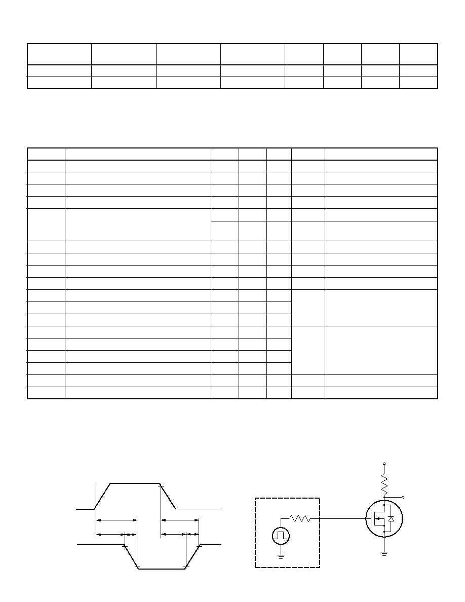
Ordering Information
BV
DSX
/
R
DS(ON)
I
DSS
BV
DGX
(max)
(min)
TO-92
TO-243AA*
Die
500V
1.0K
1.0mA
LND150N3
LND150N8
LND150ND
Order Number / Package
* Same as SOT-89. Product shipped on 2000 piece carrier tape reels.
Features
ESD gate protection
Free from secondary breakdown
Low power drive requirement
Ease of paralleling
Excellent thermal stability
Integral source-drain diode
High input impedance and low C
ISS
Applications
Solid state relays
Normally-on switches
Converters
Power supply circuits
Constant current sources
Input protection circuits
N-Channel Depletion-Mode
MOSFET
Product marking for TO-243AA:
Where
= 2-week alpha date code
LN1E
Package Options
TO-243AA
(SOT-89)
TO-92
G
S
D
S
S G D
Note: See Package Outline section for dimensions.

2
90%
10%
90%
90%
10%
10%
PULSE
GENERATOR
V
DD
R
L
OUTPUT
D.U.T.
t
(ON)
t
d(ON)
t
(OFF)
t
d(OFF)
t
F
t
r
INPUT
INPUT
OUTPUT
0V
V
DD
R
gen
0V
-10V
Thermal Characteristics
Package
I
D
(continuous)*
I
D
(pulsed)
Power Dissipation
jc
ja
I
DR
I
DRM
*
@T
A
= 25
∞
C
∞
C/W
∞
C/W
TO-92
30mA
30mA
0.74W
125
170
30mA
30mA
TO-243AA
30mA
30mA
1.6W
31
105
30mA
30mA
* I
D
(continuous) is limited by max rated T
f
.
Mounted on FR5 Board, 25mm x 25mm x 1.57mm. Significant P
D
increase possible on ceramic substrate.
LND150
Symbol
Parameter
Min
Typ
Max
Unit
Conditions
BV
DSX
Drain-to-Source Breakdown Voltage
500
V
V
GS
= -10V, I
D
= 1.0mA
V
GS(OFF)
Gate-to-Source OFF Voltage
-1.0
-3.0
V
V
DS
= 25V, I
D
= 100nA
V
GS(OFF)
Change in V
GS(OFF)
with Temperature
5.0
mV/∞C
V
DS
= 25V, I
D
= 100nA
I
GSS
Gate Body Leakage Current
100
nA
V
GS
= ±20V, V
DS
= 0V
I
D(OFF)
Drain-to-Source Leakage Current
100
nA
V
GS
= -10V, V
DS
= 450V
100
µA
V
GS
= -10V, V
DS
= 0.8V max rating
T
A
=125∞C
I
DSS
Saturated Drain-to-Source Current
1.0
3.0
mA
V
GS
= 0V, V
DS
= 25V
R
DS(ON)
Static Drain-to-Source ON-State Resistance
850
1000
V
GS
= 0V, I
D
= 0.5mA
R
DS(ON)
Change in RDS(ON) with Temperature
1.2
%/∞C
V
GS
= 0V, I
D
= 0.5mA
G
FS
Forward Transconductance
1.0
2.0
m
V
GS
= 0V, I
D
= 1.0mA
C
ISS
Input Capacitance
7.5
10
C
OSS
Output Capacitance
2.0
3.5
pF
C
RSS
Reverse Transfer Capacitance
0.5
1.0
t
d(ON)
Turn-ON Delay Time
0.09
tr
Rise Time
0.45
t
d(OFF)
Turn-OFF Delay Time
0.1
t
f
Fall Time
1.3
V
SD
Diode Forward Voltage Drop
0.9
V
V
GS
= -10V, I
SD
= 1.0mA
t
rr
Reverse Recovery Time
200
ns
V
GS
= -10V, I
SD
= 1.0mA
Notes:
1. All D.C. parameters 100% tested at 25∞C unless otherwise stated. (Pulse test: 300µs pulse, 2% duty cycle.)
2.
All A.C. parameters sample tested.
Electrical Characteristics
(@ 25∞C unless otherwise specified)
µs
V
GS
= -10V, V
DS
= 25V
f = 1 MHz
V
DD
= 25V, I
D
= 1.0mA,
R
GEN
= 25
Switching Waveforms and Test Circuit

3
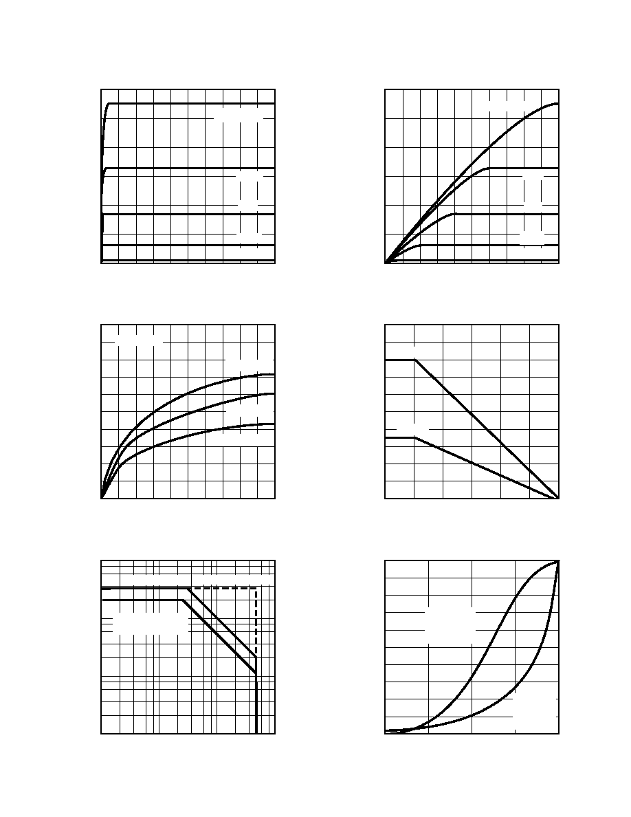
Output Characteristics
6
5
4
3
2
1
0
0
250
500
I
D
(milliamps)
Saturation Characteristics
6
5
4
3
2
1
0
0
1
2
3
5
4
Maximum Rated Safe Operating Area
1
1000
100
10
1
10
100
0.1
Thermal Response Characteristics
Thermal Resistance (normalized)
1.0
0.8
0.6
0.4
0.2
0.001
10
0.01
0.1
1.0
Transconductance vs. Drain Current
10
8
6
4
2
0
0
10
2
4
6
G
FS
(millisiemens)
Power Dissipation vs. Ambient Temperature
0
150
100
50
2
1
125
75
25
P
D
(watts)
V
DS
= 400V
V
GS
= 1.0V
0.5V
8
0V
-0.5V
-1.0V
V
GS
=1.0V
0.5V
0V
-0.5V
-1.0V
0
0
TO-243AA
V
DS
(volts)
V
DS
(volts)
I
D
(milliamps)
T
A
= -55∞C
T
A
= 25∞C
T
A
= 125∞C
I
D
(milliamps)
T
A
(∞C)
I
D
(milliamps)
V
DS
(volts)
TO-243AA (DC)
T
A
= 25∞C
TO-92 (pulsed)
TO-92 (DC)
t
P
(seconds)
TO-243AA
T
A
= 25∞C
P
D
= 1.6W
TO-92
P
D
= 1W
T
C
= 25∞C
TO-92
Typical Performance Curves
LND150

4
1235 Bordeaux Drive, Sunnyvale, CA 94089
TEL: (408) 744-0100 ∑ FAX: (408) 222-4895
www.supertex.com
12/13/010
©2001 Supertex Inc. All rights reserved. Unauthorized use or reproduction prohibited.
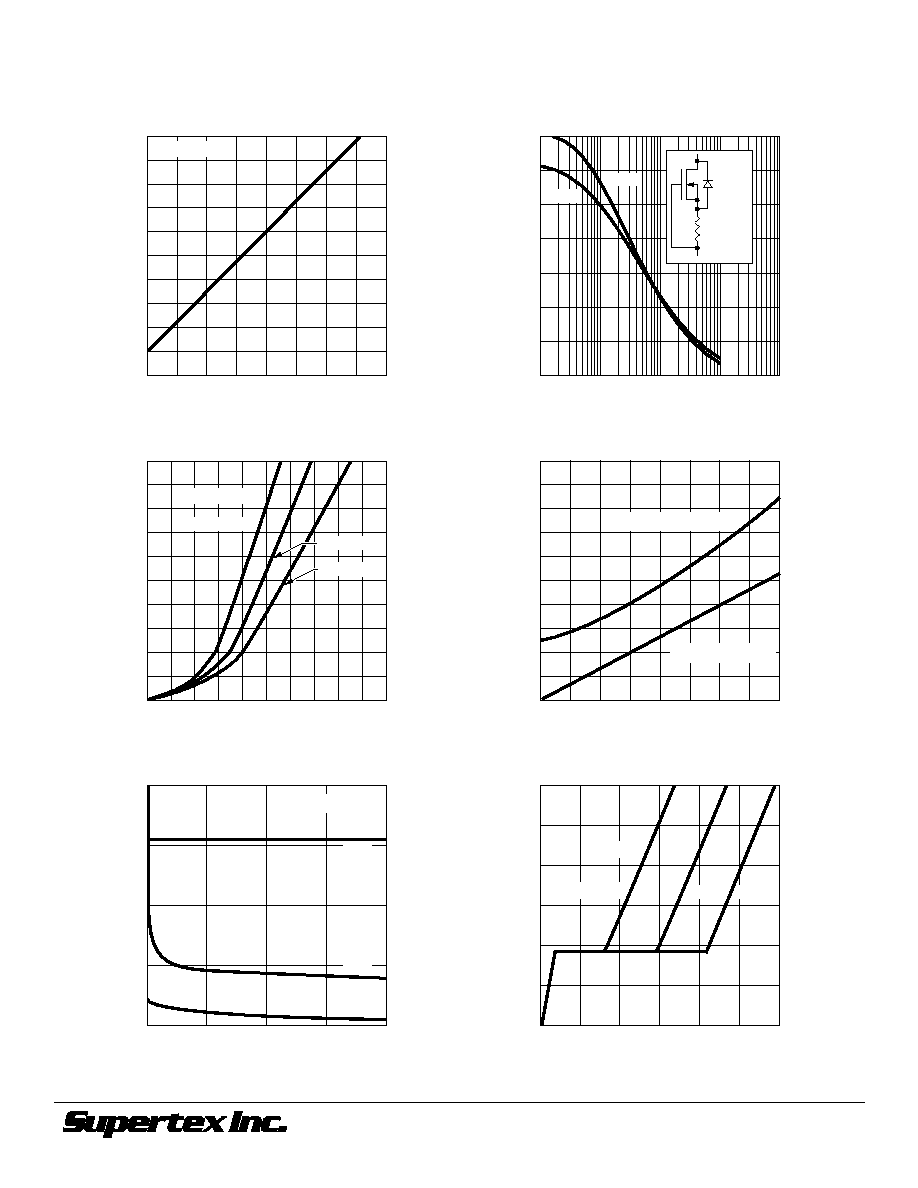
Gate Drive Dynamic Characteristics
V
GS(OFF)
and R
DS
Variation with Temperature
Transfer Characteristics
Capacitance vs. Drain-to-Source Voltage
10
C (picofarads)
0
10
20
30
40
5
-1
0
1
2
3
10
5
-50
0
50
100
150
1.1
1.8
1.6
1.4
1.2
1.0
0.8
10
5
0
-5
0
0.1
0.2
0.3
-50
0
50
100
150
T
A
= 25∞C
0
V
DS
= 400V
0.9
1.0
V
GS(OFF)
@ 100nA
R
DS(ON)
@ I
D
= 1mA
0
V
GS
= -5V
2.0
1.6
1.2
0.8
0.4
V
GS
= -10V
T
A
= 125∞C
8.7pF
60V
40V
100K
10
0.2
100
1K
10K
0.4
0.6
0.8
1.0
1.2
R
SOURCE
(ohms)
I
D
vs. R
SOURCE
1.4
0.0
LND1
I
D
R
SOURCE
BV
DSS
Variation with Temperature
BV
DSS
(normalized)
T
j
(∞C)
I
D
(milliamps)
T
A
= -55∞C
I
D
(milliamps)
V
GS
(volts)
C
ISS
C
OSS
C
RSS
V
DS
(volts)
V
GS
(volts)
T
j
(∞C)
V
DS
= 20V
Q
C
(nanocoulombs)
V
GS(OFF)
(normalized)
R
DS(ON)
(normalized)
25∞C
125∞C
Typical Performance Curves
LND150

