1
LR12
A081605
High Input Voltage
Adjustable 3-Terminal Linear Regulator
Features
13.2V to 100V Input Voltage Range
Stable with 100nF output capacitor
Adjustable 1.20V to 88V output regulation
5% reference voltage tolerance
Output current limiting, 50mA min.
10
µA typical ADJ current
Over temperature protection
Available in 3 different packages
Applications
DC/DC SMPS startup circuits
Adjustable high voltage constant current sources
Industrial Controls
Motor Controls
Battery Powered Systems
Power Supplies
Telecom Applications
LED Drivers
Automotive Applications
General Description
The Supertex LR12 is a high voltage, low output current, adjustable
linear regulator. It has a wide operating input voltage range of
13.2V to 100V. The output voltage can be adjusted from 1.20V to
88V provided that the input voltage is at least 12V greater than the
output voltage. The output voltage can be adjusted by means of
two external resistors R
1
and R
2
as shown in the typical application
circuits. The LR12 regulates the voltage difference between V
OUT
and ADJ pins to a nominal value of 1.20V. The 1.20V is amplified
by the external resistor ratio R
1
and R
2
. An internal constant bias
current of typically 10µA is connected to the ADJ pin. This
increases V
OUT
by a constant voltage of 10µA times R
2
.
The LR12 has current limiting and temperature limiting. The
output current limit is 100mA maximum and the minimum
temperature limit is 125∞C. An output short circuit current will
therefore be limited to 100mA maximum. When the junction
temperature reaches its temperature limit, the output current and/
or output voltage will decrease to keep the junction temperature
from exceeding its temperature limit. For SMPS start-up circuit
applications, the LR12 turns off when an external voltage greater
than the output voltage of the LR12 is applied to V
OUT
of the LR12.
To maintain stability, a bypass capacitor of 100nF or larger and a
minimum DC output current of 500µA are required.
The device is available in TO-92, SO-8, and TO-252 (D-PAK)
packages.
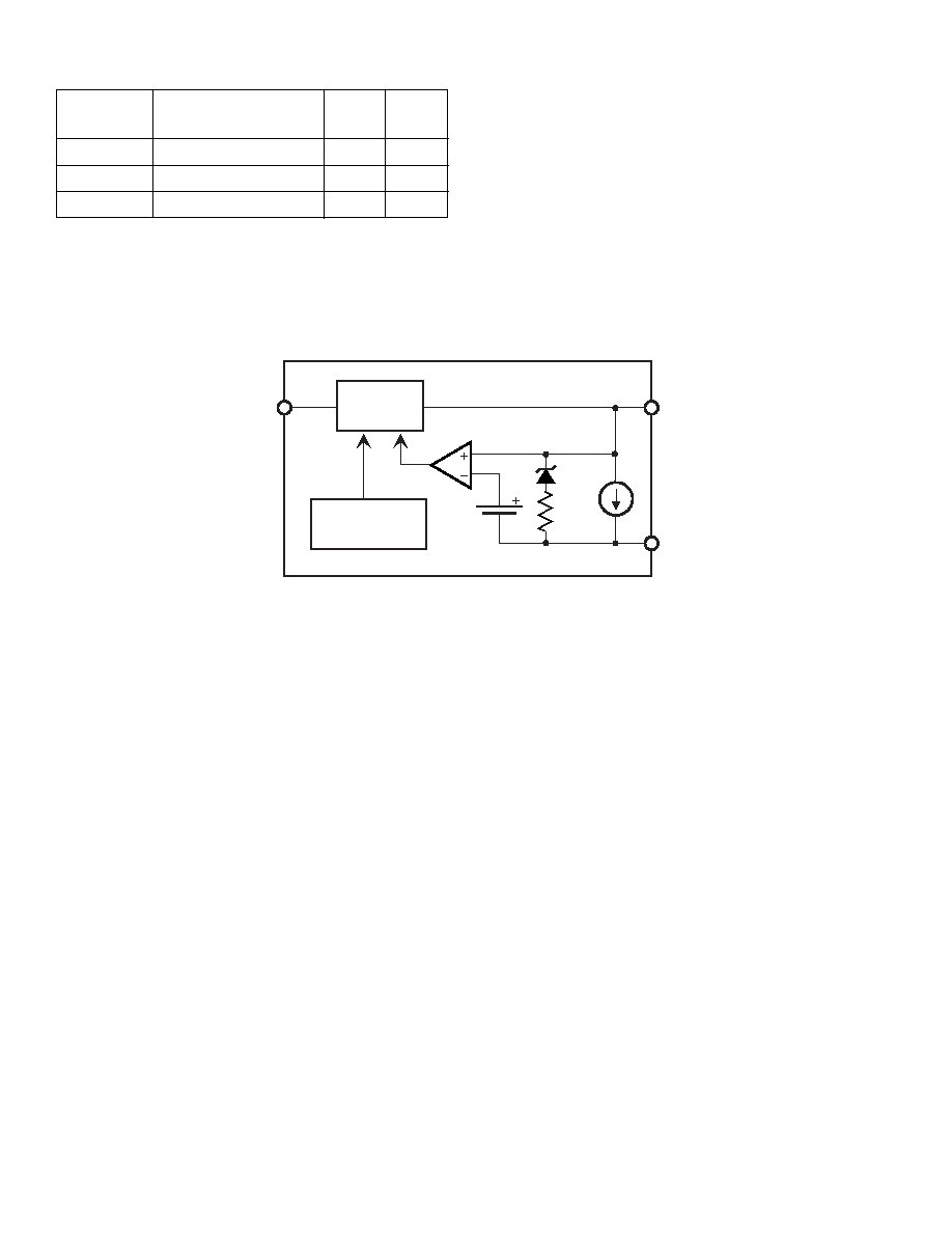
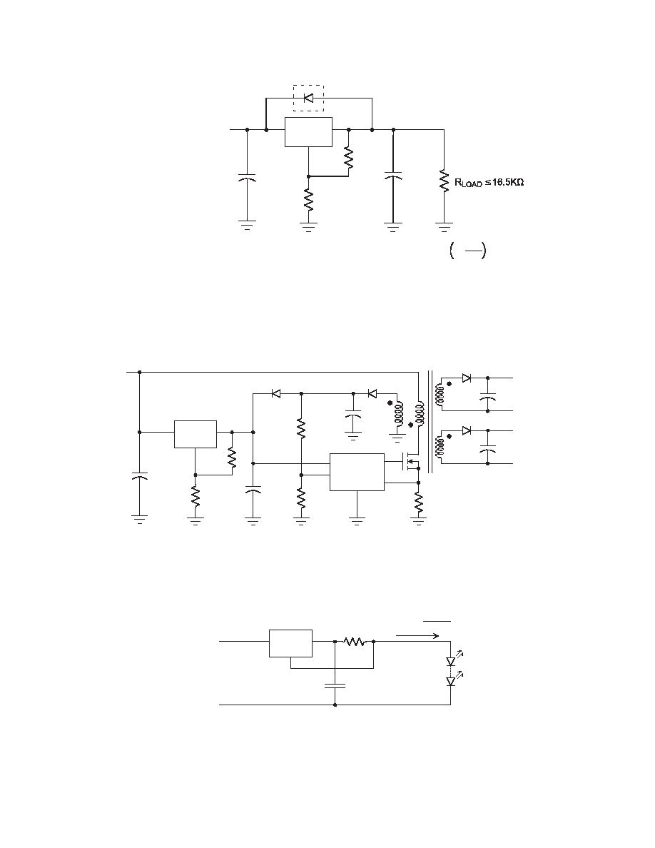
LR12 Typical Application
V
IN
V
OUT
ADJ
V
IN
*
*Required for conditions where V
IN
is less than V
OUT
.
R1
R2
C2
C1
R
LOAD
V
OUT
1.2V to 88V
13.2V to
100V
LR12
LR12
A081605
2
LR12
A081605
Package Options
SO-8
TO-252
1
TO-92
LR12LG
LR12K4
LR12N3
LR12LG-G
LR12K4-G
LR12N3-G
Ordering Information
Absolute Maximum Ratings
V
IN-ADJ
-0.5V to +120V
V
OUT-ADJ
-10V to +10V
V
IN
≠ V
OUT
-0.5V to +120V
Operating Ambient Temperature Range
-40∞C to +85∞C
Operating Junction Temperature Range
-40∞C to +125∞C
Storage Temperature Range
-65∞C to +150∞C
Pin Configurations
V
IN
ADJ
V
OUT
TO-252
(D-PAK)
SO-8
1
2
3
4
8
7
6
5
ADJ
NC
NC
V
IN
V
OUT
V
OUT
V
OUT
V
OUT
Electrical Characteristics
Test conditions unless otherwise specified: -40∞C < T
A
< 85∞C.
Symbol
Parameter
Min
Typ
Max
Units
Test Conditions
V
IN
- V
OUT
Input to Output Voltage Difference
12
98.8
V
V
OUT
Overall Output Voltage Regulation
1.14
1.20
1.26
V
13.2V<V
IN
<100V, R
1
= 2.4K
, R
2
= 0
V
OUT
Line Regulation
0.003
0.03
%/V
15V<V
IN
<100V, V
OUT
= 5V, I
OUT
= 0.5mA
V
OUT
Load Regulation
1.4
3.0
%
V
IN
= 15V, V
OUT
= 5V, 0.5mA<I
OUT
<50mA
V
OUT
Temperature Regulation
-1
+1
%
V
IN
= 15V, V
OUT
= 5V, I
OUT
= 10mA,
-40∞C<T
A
<85∞C
I
OUT
Output Current Limit
50
100
mA
T
J
< 85∞C, V
IN
- V
OUT
= 12V
I
OUT
Output Current Limit
0.5
mA
T
J
> 125∞C, V
IN
- V
OUT
= 100V
I
OUT
Minimum Output Current
0.5
mA
Includes R
1
and load current
I
ADJ
Adjust Output Current
5
10
15
µA
C2
Minimum Output Load Capacitance
100
nF
DV
OUT
/DV
IN
Ripple Rejection Ratio
50
60
dB
120Hz, V
OUT
= 5V
T
LIMIT
Junction Temperature Limit
125
∞C
TO-92
V
IN
V
OUT
ADJ
Notes:
1. TO-252 supplied on 2000 piece carrier tape reels only
-G indicates package is RoHS compliant "Green"
4
LR12
A081605
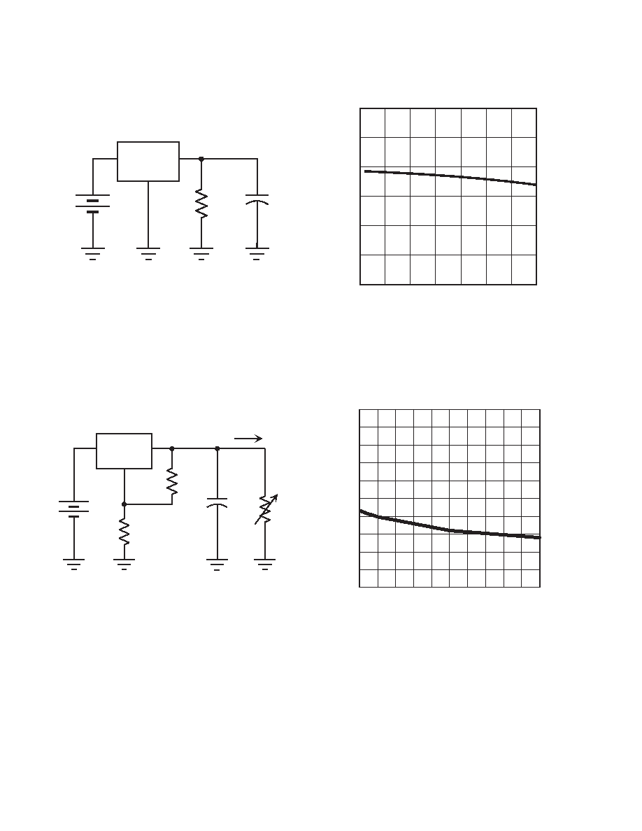
Typical Application Circuits
LR12
V
IN
= 15V
to 100V
V
OUT
ADJ
V
IN
R
I
OUT =
1.20V
R
+
-
100nF
Figure 3: High Voltage Adjustable Constant Current Source
PWM IC
LR12
Vout1
Vout2
+
+
-
-
Vcc
VAuxiliary
V
IN
=15V to 100V
V
OUT
ADJ
V
IN
FB
Figure 2: SMPS Start-Up Circuit
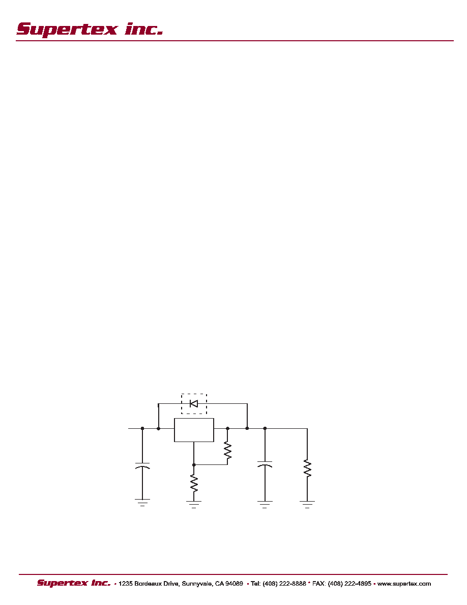
LR12
V
IN
=17V to 100V
V
OUT
ADJ
V
IN
*
R1
6.04K
±1%
R2
18.2K
±1%
C2
100nF
C1
V
OUT
=5.0V
V
OUT
= 1.20V 1+
R2
R1
+ I
ADJ
R2
Figure 1: High Input Voltage, 5.0V Output Linear Regulator
* Required for conditions where V
IN
is less than V
OUT
.