 | –≠–ª–µ–∫—Ç—Ä–æ–Ω–Ω—ã–π –∫–æ–º–ø–æ–Ω–µ–Ω—Ç: LR745N8 | –°–∫–∞—á–∞—Ç—å:  PDF PDF  ZIP ZIP |
1
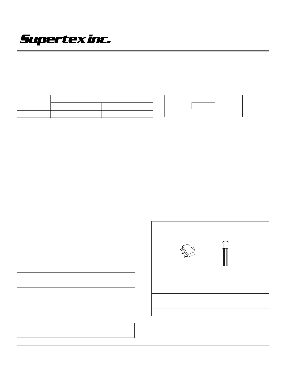
TO-243AA
(SOT-89)
Order Number / Package
TO-92
TO-243AA*
450V
LR745N3
LR745N8
*Same as SOT-89. Product supplied on 2000 piece carrier tape reels.
LR745
Ordering Information
High Input Voltage
SMPS Start-up Circuit
Maximum Input
Voltage
V
IN
GND
V
OUT
TO-92
1
2
3
TO-243AA
1
2, TAB
3
Pin Configuration
1 2 3
TO-92
1
3
2
Absolute Maximum Ratings
Input Voltage
450V
Output Voltage
25V
Operating and Storage Temperature
≠55
∞C to 150∞C
Soldering Temperature*
300
∞C
*Distance of 1.6mm from case for 10 seconds
TAB
Features
25V to 450V operating input voltage range
Compatible with industry standard PWM ICs.
See application notes AN-H28 and AN-H29.
Output current limiting
For PWM ICs with start-up threshold voltage
of 13.9V to 18.8V
Very low power consumption after start-up
Applications
Notebook and Laptop computers
Telecommunication power supplies
Battery chargers
Motor controller
General Description
The Supertex LR7 is a high input voltage SMPS start-up circuit.
The LR7 is ideally suited for use with industry standard low
voltage PWM ICs having start thresholds of 13.9V to 18.8V. It
allows the PWM ICs to be operated from rectified 120V or
240VAC lines, and eliminates the use of power resistors often
used for this purpose. The internal circuitry of the LR7 allows the
PWM ICs to operate at a V
CC
voltage below their start threshold
voltage after start-up. The auxiliary voltage can be less than the
start threshold voltage, which allows for improved efficiency.
Current from the high voltage line is drawn only during the start-
up period. After start-up, the internal high voltage line is discon-
nected from the IC thereby reducing the continuous power
dissipation to a minimum.
For detailed circuit and application information, please refer
to application notes AN-H28 and AN-H29.
Product marking for TO-243AA:
LR7
where
= 2-week alpha date code
11/12/01
Supertex Inc. does not recommend the use of its products in life support applications and will not knowingly sell its products for use in such applications unless it receives an adequate "products liability
indemnification insurance agreement." Supertex does not assume responsibility for use of devices described and limits its liability to the replacement of devices determined to be defective due to
workmanship. No responsibility is assumed for possible omissions or inaccuracies. Circuitry and specifications are subject to change without notice. For the latest product specifications, refer to the
Supertex website: http://www.supertex.com. For complete liability information on all Supertex products, refer to the most current databook or to the Legal/Disclaimer page on the Supertex website.
2
+
≠
+
+
≠
≠
comp2
Clk
Clock
Reset
Q
GND
R
D
V
OUT
V
OUT
V
IN
M2
M1
R1
R2
R3
2 to 4 mA
R4
23V
Vz
comp1
V
REF
Symbol
Parameter
Min
Typ
Max
Unit
Conditions
V
OUT
Output Voltage
18.8
24
V
I
OUT
= 0
V
OUT
over Temperature
18.5
24.3
V
I
OUT
= 0, T
A
= -40
∞C to +85∞C
I
OUT
Output Current Limiting
2
3
4
mA
V
IN
Operating Input Voltage Range
25
450
V
I
INQ
Input Quiescent Current
500
µA
V
IN
= 400V, I
OUT
= 0
V
OFF
Output Turn OFF Voltage
12.6
13.25
13.9
V
V
OFF
Over Temperature
12.3
13.25
14.2
V
T
A
= -40
∞C to +85∞C
V
RESET
Output Reset Voltage
6.3
7
7.7
V
V
RESET
Over Temperature
6
7
8
V
T
A
= -40
∞C to +85∞C
I
OFF
V
IN
Off-State Leakage Current
75
µA
V
IN
= 400V
V
AUX
External Voltage Applied to V
OUT
22
V
I
AUX
Input Current to V
OUT
500
µA
V
AUX
= 22V
Electrical Characteristics
Test conditions unless otherwise specified: T
A
= 25
∞C; V
IN
= 450V
LR745
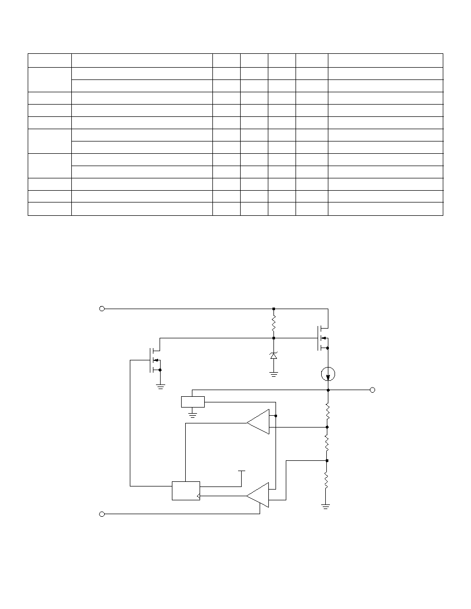
Block Diagram
3
High Voltage
V
IN
V
OUT
V
CC
I
AUX
V
AUX
C1
C2
D2
I
IN
LR7
GND
PWM IC
UC3844
LR745
Block Diagram Detailed
Description
The Supertex LR7 is a high voltage switch mode power supply
start-up circuit, which has 3 terminals: V
IN
, GND, and V
OUT
. An
input voltage range of 25VDC to 450VDC can be applied directly
at the input V
IN
pin. The output voltage, V
OUT
, is monitored by
the 2 comparators, comp1 and comp2. An internal reference,
V
REF
, and resistor divider R1, R2, and R3 set the nominal V
OUT
trip points of 7.0V for comp1 and 13.25V for comp2.
When a voltage is applied on V
IN
, V
OUT
will start to ramp up from
0V. When V
OUT
is less than 7.0V, the output of comp1 will be at
a logic high state keeping the D flip flop in a reset state. The
output of the D flip flop, Q, will be at logic low keeping transistor
M2 off. The data input for the D flip flop, D, is internally connected
to a logic high. As V
OUT
becomes greater than 7.0V, comp1 will
change to a logic low state. V
OUT
will continue to increase, and
the constant current source of typically 3mA output will charge an
external storage capacitor. As V
OUT
reaches above 13.25V, the
output of comp2, will then switch from a logic high to a logic low
state. The D flip flop's output does not change state since its
clock input is designed to trigger only on a rising edge, logic low
to logic high transition. When there is no load connected to the
output, the output voltage will continue to increase until it
reaches 21.5V which is the zener voltage minus the threshold
voltage of transistor M1. The zener voltage is typically 23V and
the threshold voltage of M1 is typically 1.5V. The zener diode is
biased by resistor R4.
V
OUT
will start to decrease when it is connected to an external
load greater than the internal constant current source, which is
the case when the PWM IC starts up. When V
OUT
falls below
13.25V, the output of comp2 will switch from a logic low to a logic
high. The output of comp2 will clock in a logic 1 into the D flip flop
causing the D flip flop's output, Q, to switch from a logic low to a
logic high. Transistor M2 will then be turned on pulling the gate
of transistor M1 to ground thereby turning transistor M1 off.
Transistor M1 will remain off as long as V
OUT
is greater than 7.0V.
Once V
OUT
decreases below 7.0V, comp1 will reset the D flip flop,
thereby turning transistor M2 off and transistor M1 back on.
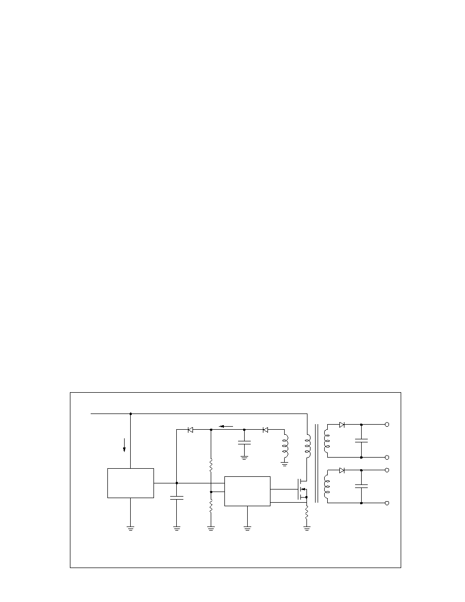
Typical Application
Figure 1 shows a simplified typical configuration of a switch
mode power supply, SMPS, using the Supertex LR7 in the start-
up circuit.
The LR7's V
OUT
terminal is connected to the V
CC
line of a PWM
IC, Unitrode part #UC3844. An auxiliary winding on the trans-
former is used to generate a V
CC
voltage to power the PWM IC
after start-up. The LR7 is used to supply power for the PWM IC
only during start-up. After start-up, the LR7 turns off and the
auxiliary winding is used to supply power for the PWM IC. Figure
2 shows the typical current and voltage waveforms at various
stages from power up to operation powered by the auxiliary
winding.
Stage I
Once a voltage is applied on V
IN
, the LR7 will start to charge the
V
CC
capacitor, C1. The V
CC
voltage will start to increase at a rate
limited by the internal current limiter of 3.0mA. The PWM IC is
in its start-up condition and will typically draw 0.5mA from the V
CC
line. The V
CC
voltage will continue to increase until it reaches the
PWM IC's start threshold voltage of typically 16V.
Stage II
Once V
CC
reaches 16V, the PWM IC is in its operating condition
and will draw typically 20mA depending on the operating fre-
quency and size of the switching MOSFET. The output of LR7,
V
OUT
, is internally current limited to 3.0mA. The remaining 17mA
will be supplied by C1 causing the V
CC
voltage decrease. When
V
CC
decreases to 13.25V, the LR7 will turn off its output thereby
reducing its input current from 3.0mA to 10's of microamperes.
At this point, all 20mA will be supplied by C1. The PWM IC can
now operate to a minimum V
CC
voltage of typically 10V.
Once the switching MOSFET starts operating, the energy in the
primary winding is transferred to the secondary outputs and the
auxiliary winding, thereby building up V
AUX
. It is necessary to
size the V
CC
storage capacitor, C1, such that V
AUX
increases to
a voltage greater than 10V before V
CC
decreases to 10V. This
allows V
AUX
to supply the required operating current for the PWM IC.
Figure 1: Simplified SMPS using LR7
(Continued on page 14-9)

4
Figure 2
LR745
0.0
3.0
2.0
1.0
0.0
12.0
8.0
4.0
0.0
30.0
20.0
10.0
0.0
4.0
PWM IC Start Threshold Voltage
LR7 V
OFF
Trip Point
Auxiliary Supply Powers PMW IC
t
t
t
t
8.0
12.0
13.5
16.0
LR7 Start-up Waveforms
V
OUT
(Volts)
I
Stage
Stage
Stage
I
IN
(mA)
V
AUX
(Volts)
I
AUX
(mA)
V
AUX
= 12V
I
AUX
= 20mA
I
IN
0mA
III
II
5
(Continued from page 14-7)
If for some reason the auxiliary voltage does not reach 10V, V
CC
will continue to decrease. Once V
CC
goes below 10V, the PWM
IC will return to its start-up condition. The PWM IC will now only
draw 0.5mA. V
CC
will continue to decrease but at a much slower
rate. Once V
CC
decrease below 7.0V, the LR7 will turn the
output, V
OUT
, back on. V
OUT
will start charging C1 as described in
Stage I.
Stage III
At this stage the LR7's output is turned off and the PWM IC is
operating from the V
AUX
supply. The auxiliary voltage, V
AUX
, can
be designed to vary anywhere between the minimum operating
V
CC
voltage of the PWM IC (10V) to the maximum auxiliary
voltage rating of the LR7 (22V).
Design Considerations
I. Calculating the value for C1
Sizing the V
CC
capacitor, C1, is an important factor. Making C1
too large will cause the SMPS to power up too slowly. However,
if too small, C1 will not allow the SMPS to power up due to
insufficient charge in the capacitor to power the IC and MOSFET
until the auxiliary supply is available. The value of C1 can be
approximately by the following equation:
C1
1
f
N
l
V
V
START
MIN
=
◊
( )
◊
( )
-
(
)
where,
f
=
switching frequency
N
=
number of clock cycles required to charge
V
AUX
to V
MIN
value
I
=
PWM operating current
V
START
=
PWM IC start threshold rating
V
MIN
=
PWM IC minimum V
CC
operating voltage
Consider for example, a PWM IC with a switching frequency of
100KHz, operating current of 20mA, start threshold of 16V, and
a minimum operating voltage of 10V. If 100 clock cycles are
required to charge the auxiliary voltage to 10V, the minimum
value of C1 is calculated as follows:
C1=
1
100KHZ
100
20mA
16V -10V
◊
( )
◊
(
)
(
)
C1= 3.3
µF
II. SMPS with wide minimum to maximum load
An important point is that the LR7's output voltage, V
OUT
, must
discharge to below the nominal V
OFF
trip point of 13.25V in order
for its output to turn off. If the SMPS requires a wide minimum
to maximum output load variation, it will be difficult to guarantee
that V
CC
will fall below 13.25V under minimum load conditions.
Consider an SMPS that is required to power small as well as
large loads and is also required to power up quickly. Such as
SMPS may power up too fast with a small load, not allowing the
V
CC
voltage to fall below 13.25V. For such conditions, the circuit
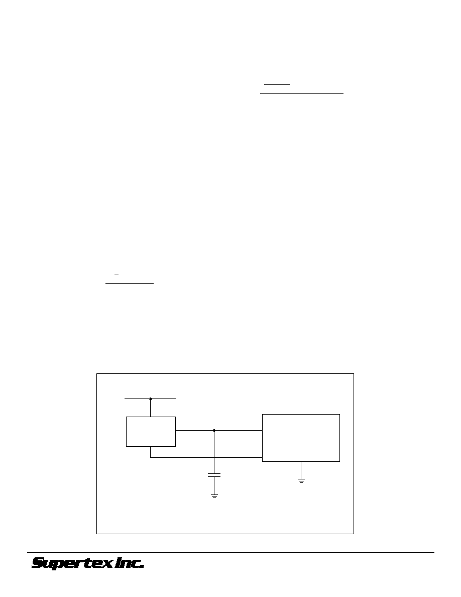
in Figure 3 is recommended.
In Figure 3, the V
REF
pin of the UC3844 is used to bias the ground
pin of the LR7. The V
REF
pin on the UC3844 is a 5.0V reference,
which stays at 0V until the V
CC
voltage reaches the start thresh-
old voltage. Once V
CC
reaches the start threshold voltage, V
REF
will switch digitally from 0V to 5.0V. During start-up, the LR7 will
be on and V
CC
will start to increase up to 16V. Once V
CC
reaches
16V, the UC3844 will start to operate and V
REF
will increase from
0V to 5.0V. The LR7 will see an effective V
OUT
voltage of 11V
(16V minus 5.0V) because the ground of the LR7 is now at 5.0V.
The LR7 will immediately turn off its output V
OUT
without having
to wait for the V
CC
voltage to decrease. The V
REF
switching from
0 to 5V during start is a common feature in most PWM ICs.
LR745
LR7
PWM IC
UC3844
GND
V
IN
V
OUT
V
CC
V
REF
C1
Figure 3: Using V
REF
for the LR7 Ground Voltage
1235 Bordeaux Drive, Sunnyvale, CA 94089
TEL: (408) 744-0100 ∑ FAX: (408) 222-4895
www.supertex.com
11/12/01
©2001 Supertex Inc. All rights reserved. Unauthorized use or reproduction prohibited.