1
LR8
High Input Voltage
Adjustable 3-Terminal Linear Regulator
Features
12V to 450V input voltage range
Adjustable 1.20V to 440V output regulation
5% output voltage tolerance
Output current limiting
10
µ
A typical ADJ current
Internal junction temperature limiting
Applications
Off-line SMPS startup circuits
Adjustable high voltage constant current source
Industrial Controls
Motor controls
Battery chargers
Power supplies
General Description
The Supertex LR8 is a high voltage, low output current, adjustable
linear regulator. It has a wide operating input voltage range of
12V to 450V. The output voltage can be adjusted from 1.20V to
440V provided that the input voltage is at least 10V greater than
the output voltage. The output voltage can be adjusted by means
of two external resistors R1 and R2 as shown in the typical
application circuits. The LR8 regulates the voltage difference
between V
OUT
and ADJ pins to a nominal value of 1.20V. The
1.20V is amplified by the external resistor ratio R1 and R2. An
internal constant bias current of typically 10
µ
A is connected to
the ADJ pin. This increases V
OUT
by a constant voltage of 10
µ
A
times R2.
The LR8 has current limiting and temperature limiting. The
output current limit is typically 15mA and the minimum temperature
limit is 125
∞
C. An output short circuit current will therefore be
limited to 15mA. When the junction temperature reaches its
temperature limit, the output current and/or output voltage will
decrease to keep the junction temperature from exceeding its
temperature limit. For SMPS start-up circuit applications, the
LR8 turns off when an external voltage greater than the output
voltage of the LR8 is applied to V
OUT
of the LR8. To maintain
stability, a bypass capacitor of 1.0
µ
F or larger and a minimum DC
output current of 500
µ
A are required.
The device is available in TO-92, TO-243AA (SOT-89), and
TO-252 (D-PAK) packages.
LR8
12/03/01
Supertex Inc. does not recommend the use of its products in life support applications and will not knowingly sell its products for use in such applications unless it receives an adequate "products liability
indemnification insurance agreement." Supertex does not assume responsibility for use of devices described and limits its liability to the replacement of devices determined to be defective due to
workmanship. No responsibility is assumed for possible omissions or inaccuracies. Circuitry and specifications are subject to change without notice. For the latest product specifications, refer to the
Supertex website: http://www.supertex.com. For complete liability information on all Supertex products, refer to the most current databook or to the Legal/Disclaimer page on the Supertex website.
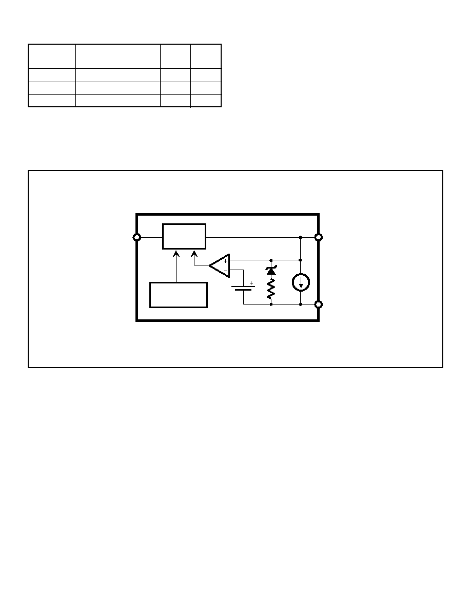
LR8 Block Diagram and Typical Application
LR8
V
IN
V
OUT
ADJ
V
IN
*
*Required for conditions where V
IN
is less than V
OUT
.
R1
R2
C2
C1
R
LOAD
VOUT
2
LR8
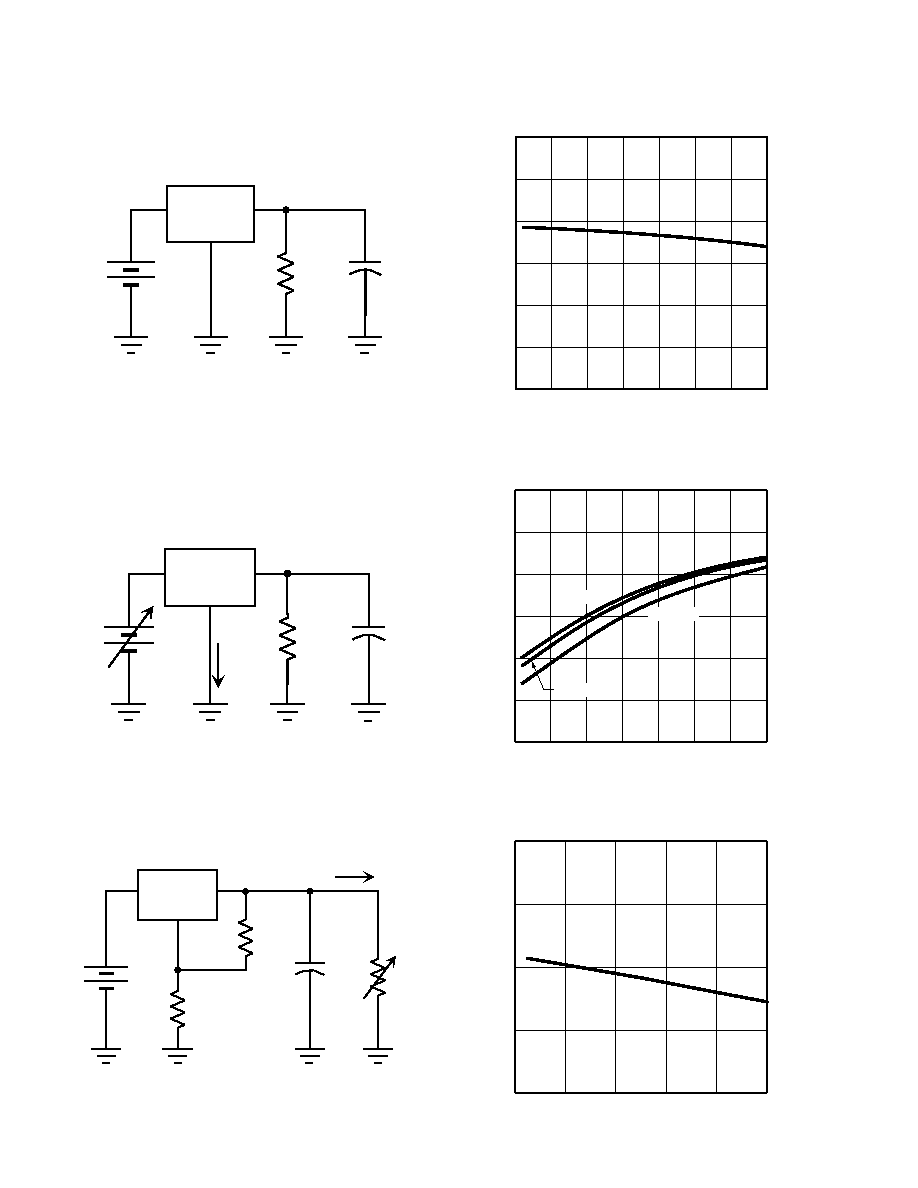
Electrical Characteristics
Test conditions unless otherwise specified: -40
∞
C < T
A
< 85
∞
C.
Symbol
Parameter
Min
Typ
Max
Units
Test Conditions
V
IN
- V
OUT
Input to Output Voltage Difference
12
450
V
V
OUT
Overall Output Voltage Regulation
1.14
1.20
1.26
V
12V<V
IN
<400V, R1=2.4K
, R2=0
V
OUT
Overall Output Voltage Regulation
375
400
425
V
R1=2.4K
, R2=782K
V
OUT
Line Regulation
0.003
0.01
%/V
15V<V
IN
<400V, V
OUT
=5V, I
OUT
=0.5mA
V
OUT
Load Regulation
1.4
3.0
%
V
IN
=15V, V
OUT
=5V, 0.5mA<I
OUT
<10mA
V
OUT
Temperature Regulation
-1
+1
%
V
IN
=15V, V
OUT
=5V, I
OUT
=10mA,
-40
∞
C<T
A
<85
∞
C
I
OUT
Output Current Limit
10
20
mA
T
J
< 85
∞
C, V
IN
- V
OUT
= 10V
I
OUT
Output Current Limit
0.5
mA
T
J
> 125
∞
C, V
IN
- V
OUT
= 450V
I
OUT
Minimum Output Current
0.3
0.5
mA
Includes R1 and load current
I
ADJ
Adjust Output Current
5
10
15
µ
A
C2
Minimum Output Load Capacitance
1
µ
F
DV
OUT
/DV
IN
Ripple Rejection Ratio
50
60
dB
120Hz, V
OUT
= 5V
T
LIMIT
Junction Temperature Limit
125
∞
C
Product marking for TO-243AA:
LR8
where
= 2-week alpha date code
Ordering Information
Absolute Maximum Ratings
V
IN
Input Voltage
-0.5V to +480V*
Output Voltage Range
-0.5V to +470V
Operating Ambient Temperature Range
-40
∞
C to +85
∞
C
Operating Junction Temperature Range
-40
∞
C to +125
∞
C
Storage Temperature Range
-65
∞
C to +150
∞
C
*Voltages referenced to ADJ.
V
IN
V
OUT
ADJ
TO-92
1
2
3
TO-243AA
1
2, TAB
3
TO-252
1
2 (TAB)
3
Pin Configurations
1
3
2
TAB
1 2 3
TO-92
1
3
2 (TAB)
TO-252
(D-PAK)
*
Same as SOT-89. Product supplied on 2000 piece carrier tape reels.
Package Options
TO-92
TO-243AA*
TO-252
LR8N3
LR8N8
LR8K4
TO-243AA
(SOT-89)
4
LR8
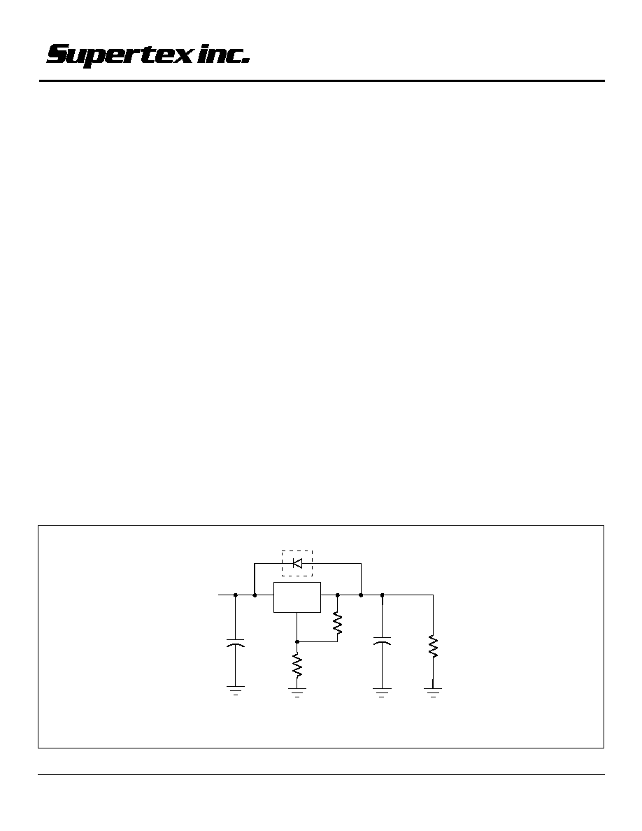
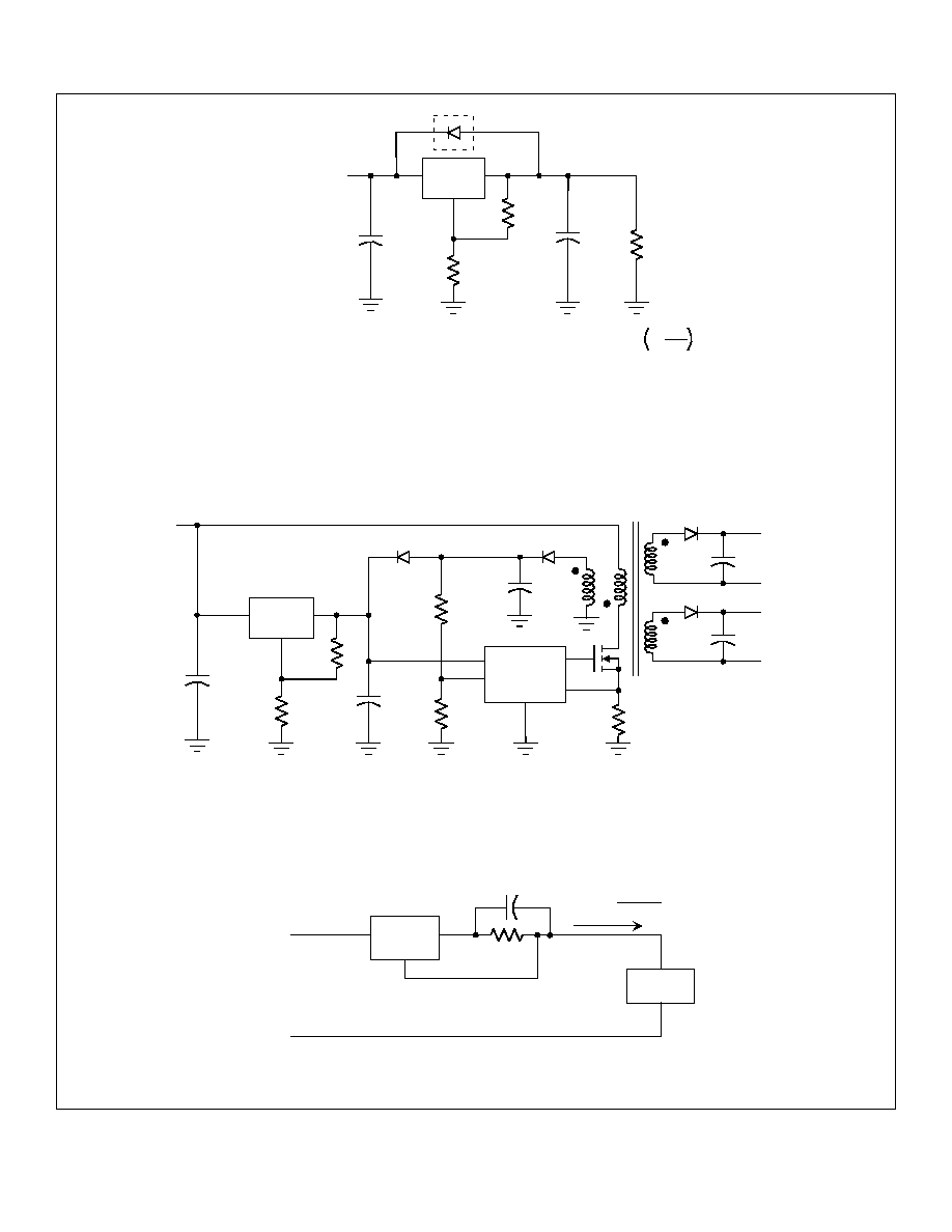
Typical Application Circuits
LR8
V
IN
=15V to 450V
V
OUT
ADJ
V
IN
*
R1
6.04K
±
1%
R2
18.2K
±
1%
C2
1.0
µ
F
C1
R
LOAD
16.5K
VOUT=5.0V
VOUT = 1.20V 1+
R2
R1
+ IADJR2
PWM IC
LR8
Vout1
Vout2
+
+
-
-
Vcc
VAuxiliary
V
IN
=15V to 450V
V
OUT
ADJ
V
IN
FB
LR8
V
IN
= 15V
to 450V
V
OUT
ADJ
V
IN
R
Load
I
OUT =
1.20V
R
+
-
1µF
Figure 1: High Input Voltage, 5.0V Output Linear Regulator
* Required for conditions where V
IN
is less than V
OUT
.
Figure 2: SMPS Start-Up Circuit
Figure 3: High Voltage Adjustable Constant Current Source