 | –≠–ª–µ–∫—Ç—Ä–æ–Ω–Ω—ã–π –∫–æ–º–ø–æ–Ω–µ–Ω—Ç: MD1211 | –°–∫–∞—á–∞—Ç—å:  PDF PDF  ZIP ZIP |
1
NR011806
MD1211
New Release
Features
10ns average rise and fall time with 1000pF load
2.0A peak output source/sink current
1.2V to 5.0V input CMOS compatible
4.5V to 13V total supply voltage
Dual matched channels
Reduced clock skew
Low input capacitance
Green packaging
Applications
Medical ultrasound imaging
Piezoelectric transducer drivers
Nondestructive evaluation
PIN diode driver
High speed level translator
Clock/line drivers
General Description
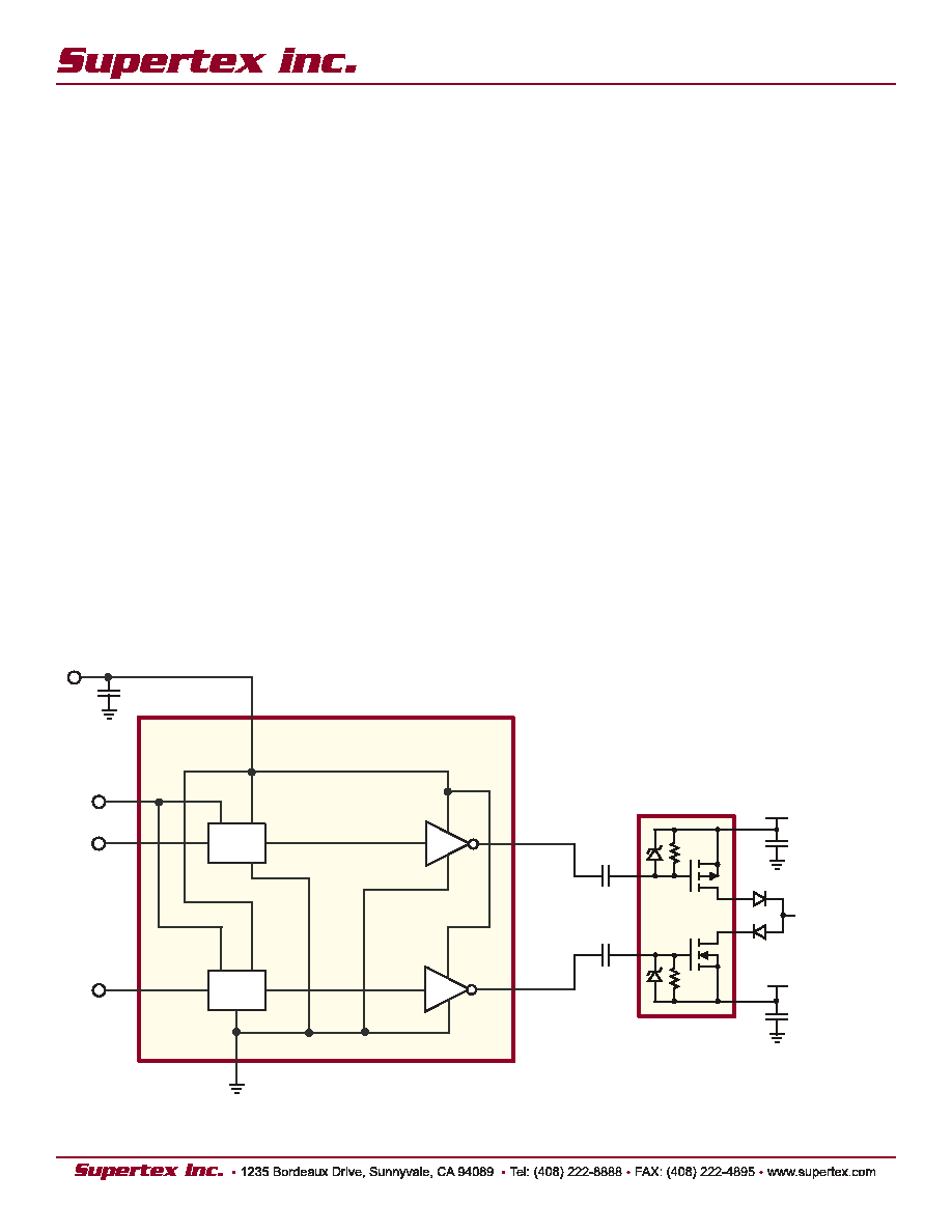
The Supertex MD1211 is a high speed, dual MOSFET driver.
It is designed to drive high voltage N- and P-channel MOSFET
transistors for medical ultrasound and other applications
requiring a high output current for a capacitive load. The
high-speed input stage of the MD1211 can operate from 1.2
to 5.0 volt logic interface with an optimum operating input
signal range of 1.8 to 3.3 volts. The level translator uses a
proprietary circuit, which provides DC coupling together with
high-speed operation.
Typical Application Circuit
High Speed, Dual MOSFET Driver
Level
Shifter
Level
Shifter
GND
V
DD
IN
B
IN
A
OUT
B
OUT
A
V
LL
MD1211
Supertex
TC6320TG
1µF
+100V
1µF
-100V
10nF
10nF
To
Piezoelectric
Transducer
0.47µF
2
NR011806
MD1211
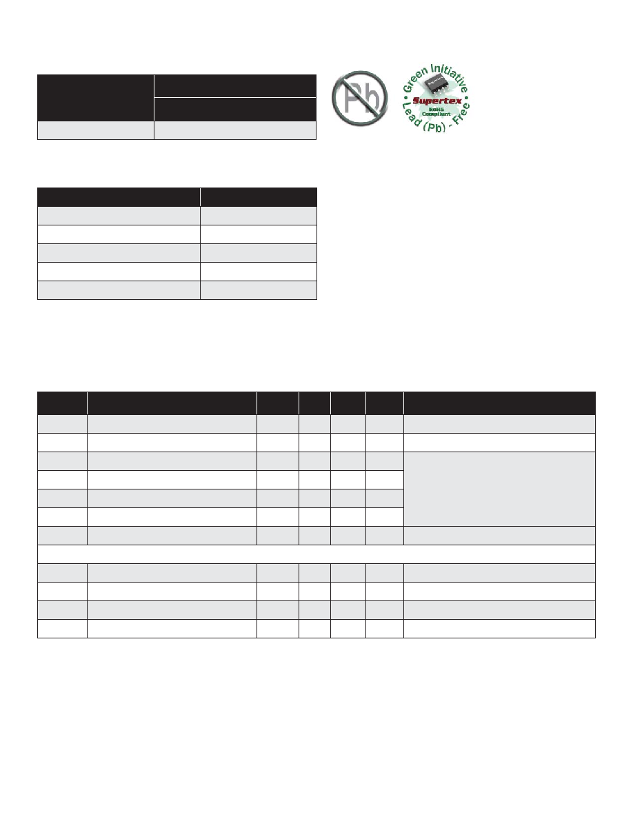
Ordering Information
DEVICE
Package Option
8-Pin SOIC
MD1211
MD1211LG-G
-G indicates package is RoHS compliant (`Green')
Absolute Maximum Ratings
Symbol
Parameter
Min
Typ
Max
Units
Conditions
V
DD
Main supply voltage
4.5
-
13
V
---
V
LL
Logic supply voltage
1.2
-
5.0
V
---
V
IH
Input logic voltage high
V
LL
-0.3
-
V
LL
V
For Logic Inputs IN
A
and IN
B
V
IL
Input logic voltage low
0
-
0.8
V
I
IH
Input logic current high
-
-
10
A
I
IL
Input logic current low
-
-
10
A
C
IN
Logic input capacitance
-
5.0
10
pF
All Inputs
Outputs
R
SINK
Output sink resistance
-
-
12
I
SINK
= 50mA
R
SOURCE
Output source resistance
-
-
12
I
SOURCE
= 50mA
I
SINK
Peak output sink current
-
2.0
-
A
---
I
SOURCE
Peak output source current
-
2.0
-
A
---
DC Electrical Characteristics
(Over operating conditions unless otherwise specifi ed, V
DD
= 12V, T
J
= 25∞C)
Parameter
Value
Logic Supply Voltage
-0.5V to +5.5V
Main Supply Voltage
-0.5V to +13.5V
Logic Input Levels
-0.5V to V
LL
+0.5V
Maximum Junction Temperature
+125∞C
Storage Temperature
-65∞C to 150∞C
Absolute Maximum Ratings are those values beyond which damage to the
device may occur. Functional operation under these conditions is not implied.
Continuous operation of the device at the absolute rating level may affect
device reliability. All voltages are referenced to device ground.
3
NR011806
MD1211
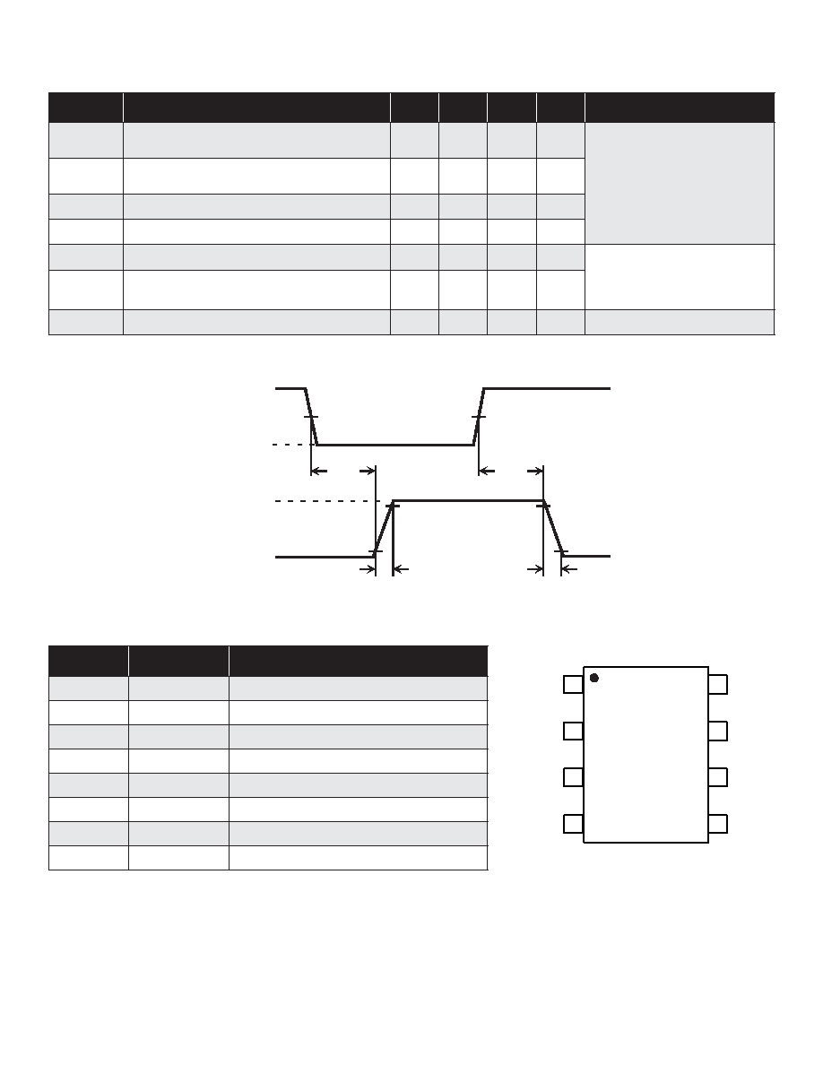
IN
t
PLH
10%
9
0
%
5
0
%
5
0
%
OUT
t
PHL
t
r
90%
10%
t
f
3.3V
0V
0V
Timing Diagram
Symbol
Parameter
Min
Typ
Max
Units
Conditions
t
PLH
Propagation delay when output is from
low to high
-
10
-
ns
C
LOAD
= 1000pF, (see timing
diagram)
Input signal rise/fall time 2ns
t
PHL
Propagation delay when output is from
high to low
-
10
-
ns
t
r
Output rise time
-
10
-
ns
t
f
Output fall time
-
10
-
ns
l t
r
- t
f
l
Rise and fall time matching
-
2.0
-
ns
For each channel
l
t
PLH
-t
PHL
l
Propagation low to high and high to low
matching
-
2.0
-
ns
t
dm
Propagation delay match
-
3.0
-
ns
Device to device delay match
AC Electrical Characteristics
Pin #
Function
Description
1
V
LL
Logic supply voltage
2
IN
A
Logic input
3
GND
Device ground
4
IN
B
Logic input
5
OUT
B
Output driver
6
V
DD
Main supply voltage
7
OUT
A
Output driver
8
V
DD
Main supply voltage
Pin Description
1
2
3
4
8
7
6
5
V
LL
GND
IN
A
IN
B
OUT
B
V
DD
OUT
A
V
DD
MD1211
4
Doc.# DSFP - MSD1211
NR011806
MD1211
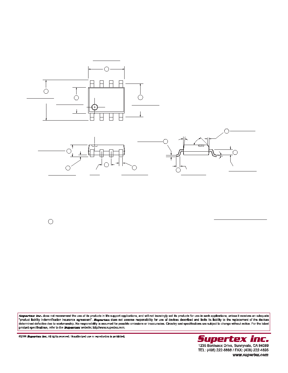
0
∞ - 8 ∞
45
∞
7
∞ (4 PLCS)
0.193
± 0.012
(4.9022
± 0.3048)
D
0.192
± 0.005
(4.8895
± 0.1143)
H
1
0.154
± 0.004
(3.9116
± 0.1016)
E
0.236
± 0.008
(5.9944
± 0.2032)
H
0.061
± 0.008
(1.5494
± 0.2032)
A
0.007
± 0.003
(0.1778
± 0.0762)
A
1
TYP.
0.050
(1.270)
e
0.016
± 0.002
(0.4064
± 0.0508)
B
C
0.010
± 0.002
(0.254
± 0.0508)
0.035
± 0.015
(0.889
± 0.381)
L
h
0.020
± 0.009
(0.508
± 0.2286)
L
1
0.0275
± 0.0025
(0.6985
± 0.0635)
Note: Circle (e.g. B ) indicates JEDEC Reference.
Dimensions in Inches
(Dimensions in Millimeters)
Measurement Legend =
8-LEAD SMALL OUTLINE PACKAGE (SOIC) (LG)