 | –≠–ª–µ–∫—Ç—Ä–æ–Ω–Ω—ã–π –∫–æ–º–ø–æ–Ω–µ–Ω—Ç: MD1711FG | –°–∫–∞—á–∞—Ç—å:  PDF PDF  ZIP ZIP |
MD1711
Rev.12 011005
1
Initial Release
High Speed, Integrated Ultrasound Driver IC
Features
Drives two ultrasound transducer channels
Generates 5-level waveform
Drives 12 high voltage MOSFETs
±2.0A source and sink peak current
Up to 20MHz output frequency
12V/ns slew rate
±3ns matched delay times
Second harmonic is less than -40dB
Two separate gate drive voltages
1.8V to 3.3V CMOS logic interface
Applications
Medical ultrasound imaging
Piezoelectric transducer drivers
Metal flaw detection
Nondestructive evaluation
Sonar Transmitter
General Description
The Supertex MD1711 is an IC for a two-channel, 5-
level, high voltage and high-speed transmitter driver.
It is designed for medical ultrasound imaging
applications but can also be used for metal flaw
detection, nondestructive evaluation, and driving
piezoelectric transducers.
The MD1711 is a two-channel logic controller circuit
with low impedance MOSFET gate drivers. There are
two sets of control logic inputs, one for channel A and
one for Channel B. Each channel consists of three
pairs of MOSFET gate drivers. These drivers are
designed to match the drive requirements of the
Supertex TC6320. The MD1711 drives six TC6320s.
Each pair an N-channel and a P-channel MOSFET.
They are designed to have the same impedance and
can provide peak currents of over 2.0 amps
.
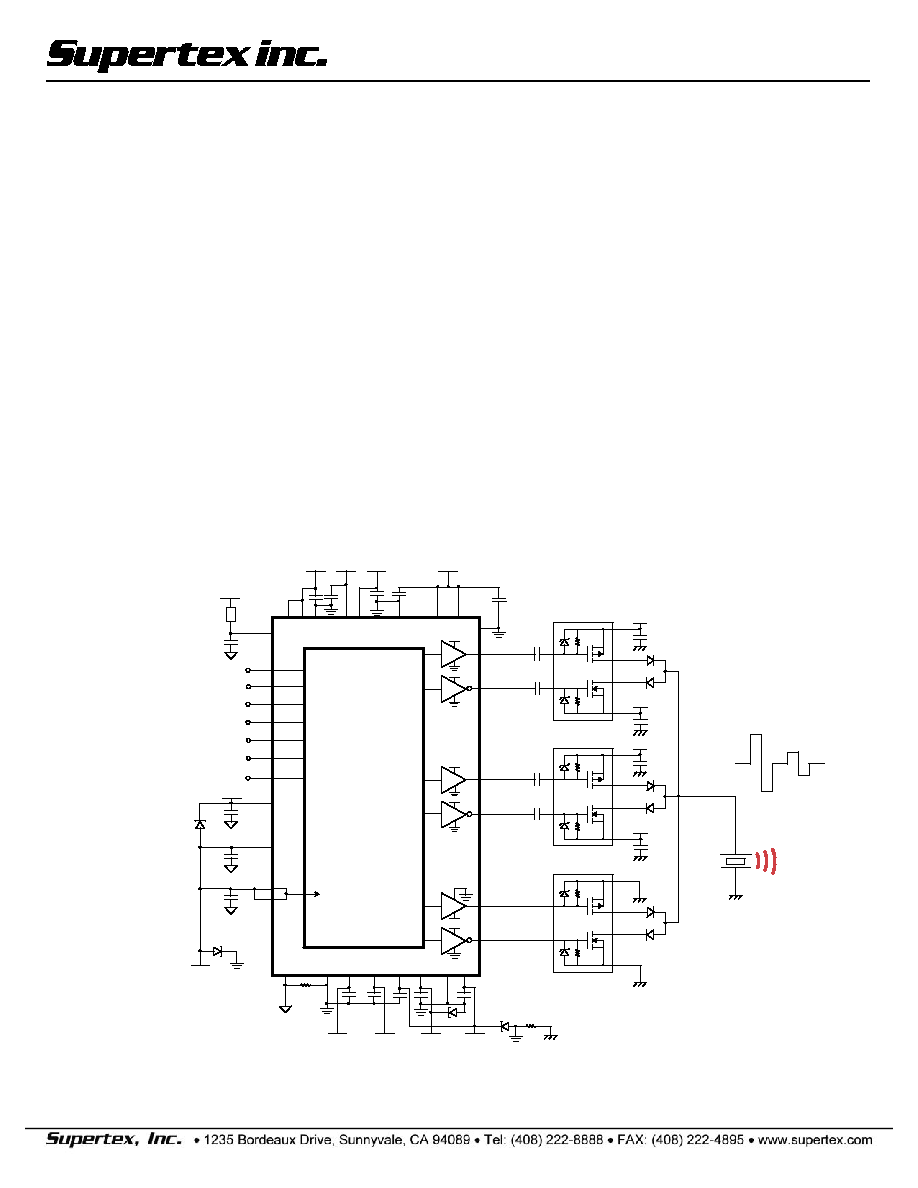
Typical Application Circuit (1 of 2 Channels)
NR012505
V
NN
1
TC6320
+100V
-100V
+50V
-50V
0V
0V
30
32
34
44
39
41
37
DV DD2
DV DD2
DV DD1
DV DD1
V
SS
DV DD1
D
VSS
-10V
DV
DD
1
DV
DD
2
16
19
21
+10V
VL L
+3 .3 V
AV S S
48
14
15
AV
SS
SEL
POSA / POS1A
EN
DGND
AGND
0
MD1711
(1/2 of I/O)
SU B
7
18
AV S S
33
36
28
25
31
DGND
35
40
42
43
DV
SS
45
FB
AV
DD
1
6
0
46
47
13
1
2
3
4
5
OUTPA1
OUTNA1
OUTPA2
OUTNA2
OUTPA3
OU
TNA3
DGND
DGND
+5V
DV
DD
1
+1 0 V
DV
DD
2
+5 V
+10V
+1 0 V
26
DGND
+10V
-10V
-1 0 V
DV
DD
2
DV
DD
1
DV
DD
1
Transducer
0.22
µF
Control Logic
& Level
Translator
NEGA / NEG1A
HVEN1A / POS2A
HVEN2A / NEG2A
ClampA
0.1
µ
F
0.1
µ
F
0.1
µ
F
0.22
µ
F
0.22
µ
F
0.22
µ
F
0.22
µ
F
0.22
µ
F
0.1
µ
F
10nF
10nF
10nF
10nF
1
µ
F
1
µ
F
1
µ
F
1
µ
F
V
NN
2
V
PP
2
V
PP
1
MD1711
NR012505
2
Ordering Information
Package Option
48 Lead LQFP
MD1711FG
Absolute Maximum Ratings*
V
LL
, Logic Supply
-0.5V to +5.5V
AV
DD
1, DV
DD
1, Positive Gate Drive Supply
-0.5V to +15V
DV
DD
2, Positive Gate Drive Supply
-0.5V to +15V
AV
SS
, DV
SS
Negative Gate Drive Supply
-15V to +0.5V
Storage temperature
-65∞C to 150∞C
Junction temperature
125∞C
LQFP Power Dissipation
1.2W
*Absolute Maximum Ratings are those values beyond which damage to the device may occur. Functional
operation under these conditions is not implied. Continuous operation of the device at the absolute rating level
may affect device reliability. All voltages are referenced to device ground.
Operating Supply Voltages and Currents
(Over operating conditions unless otherwise specified, AV
DD
1=DV
DD
1=DV
DD
2=10V, AV
SS
=DV
SS
=-10V, V
LL
=3.3V, T
A
= 25∞C)
Sym Parameter
Min Typ Max
Units
Note
V
LL
Logic
Supply
+1.8
+3.3
+5.5 V
AV
DD
1
Positive Drive Bias Supply
+8.0
+10
+12.6
V
DV
DD
1
Positive Gate Drive Supply
+4.75
+12.6
V
DV
DD
2
Positive Gate Drive Supply
+4.75
+12.6
V
AV
SS
,
DV
SS
Negative Gate Drive and
Bias Supply
-12.0 -10 -8.0 V
I
VLL
Logic Supply Current
2.0
mA
I
AVDD1
Positive Bias Current
5.0
mA
I
AVSS
&
I
DVSS
Negative Drive and Bias
Supply Current
20
mA
I
DVDD1
Positive Drive Current 1
55
mA
All channel on at 5.0Mhz, No load
I
DVDD2
Positive Drive Current 2
13
mA
DV
DD
2 = 5.0V, All channel on at
5.0Mhz, No load
I
AVDD1Q
V
AVDD1
quiescent current
2.0
mA
I
AVSSQ
V
AVSS
quiescent current
0.75
mA
I
DVDD1Q
V
DVDD1
quiescent current
10
µ
A
I
DVDD2Q
V
DVDD2
quiescent current
10
µ
A
I
VLLQ
Logic Supply Current
1.0
mA
EN = low, All inputs low or high.
JA
Thermal resistance to air
50
∞C/W 1oz. 4-layer 3x4inch PCB
MD1711
NR012505
3
DC Electrical Characteristics
(Over operating conditions unless otherwise specified, AV
DD
1=DV
DD
1=DV
DD
2=10V, AV
SS
=DV
SS
=-10V, V
LL
=3.3V, T
A
= 0 to 70∞C)
P-Channel Gate Driver Outputs
Sym Parameter
Min
Typ
Max
Units Conditions
R
SINK
Output sink resistance
6.0
I
SINK
=100mA
R
SOURCE
Output source resistance
6.0
I
SOURCE
=100mA
I
SINK
Peak output sink current
2.0
A
I
SOURCE
Peak output source current
2.0
A
N-Channel Gate Driver Outputs
Sym Parameter
Min
Typ
Max
Units Conditions
R
SINK
Output sink resistance
10
I
SINK
=100mA
R
SOURCE
Output source resistance
10
I
SOURCE
=100mA
I
SINK
Peak output sink current
1.5
A
I
SOURCE
Peak output source current
1.5
A
Logic Inputs
Sym Parameter
Min
Typ
Max
Units Conditions
V
IH
Input logic high voltage
0.8V
LL
V
LL
V
V
IL
Input logic low voltage
0
0.2V
LL
V
I
IH
Input logic high current
1.0
µA
I
IL
Input logic low current
-1.0
µA
AC Electrical Characteristics
(Over operating conditions unless otherwise specified, AV
DD
1=DV
DD
1=DV
DD
2=10V, AV
SS
=DV
SS
=-10V, V
LL
=3.3V, T
A
= 0 to 70∞C)
Sym Parameter
Min Typ Max Units Conditions
f
OUT
Output frequency range
20
MHz
t
PH
Propagation delay when output
is from low to high
19
ns
No load, See timing diagram
t
PL
Propagation delay when output
is from high to low
19
ns
No load, See timing diagram
tr
Output rise time
8.0
ns
1000pF load, see timing diagram
tf
Output fall time
8.0
ns
1000pF load, see timing diagram
t
dm
Delay time matching
±3.0
ns
No load, From device to device
t
DLAY
Output jitter
30
ps
Standard deviation of t
d
samples (1k)
SR
Output slew rate
12
V/ns
HD2 2
nd
harmonic distortion
-40
dB
Measured at TC6320 output with
100
Load
Power-Up Sequence
1 AV
SS
, DV
SS
Negative Gate Drive Supply and Substrate Bias
2 V
LL
, AV
DD
1, DV
DD
1 & DV
DD
2 Logic Supply, Positive Gate Drive Supply and Bias
MD1711
NR012505
4
Truth Table for Channels A and B (For SEL = L)
Logic Control Inputs
V
PP
1 to V
NN
1 Output
V
PP
2 to V
NN
2 Output
V
PP
3 to V
NN
3 Output
SEL EN HVEN1/
POS2
HVEN2/
NEG2
Clamp POS/
POS1
NEG/
NEG1
HV
OUT
P1 HV
OUT
N1 HV
OUT
P2 HV
OUT
N2 HV
OUT
P3
HV
OUT
N3
0
1
0 0 0
0
0
ON ON
0
1
0 0 0
0
1
ON ON
0
1
0 0 0
1
0
ON ON
0
1
0 0 0
1
1
OFF OFF
OFF OFF
0
1
0 0 1
0
0
0
1
0 0 1
0
1
0
1
0 0 1
1
0
0
1
0 0 1
1
1
OFF OFF OFF
0
1
0 1 0
0
0
OFF
OFF
ON ON
0
1
0 1 0
0
1
OFF
ON
OFF
OFF
0
1
0 1 0
1
0
ON
OFF
OFF
OFF
0
1
0 1 0
1
1
OFF
OFF OFF OFF OFF
0
1
0 1 1
0
0
0
1
0 1 1
0
1
0
1
0 1 1
1
0
0
1
0 1 1
1
1
OFF OFF OFF
0
1
1 0 0
0
0
OFF
OFF
ON ON
0
1
1 0 0
0
1
OFF
ON
OFF
OFF
0
1
1 0 0
1
0
ON
OFF OFF
OFF
0
1
1 0 0
1
1
OFF
OFF
OFF
OFF OFF
0
1
1 0 1
0
0
0
1
1 0 1
0
1
0
1
1 0 1
1
0
0
1
1 0 1
1
1
OFF OFF OFF
0
1
1 1 0
0
0
0
1
1 1 0
0
1
0
1
1 1 0
1
0
0
1
1 1 0
1
1
OFF OFF OFF
0
1
1 1 1
0
0
0
1
1 1 1
0
1
0
1
1 1 1
1
0
0
1
1 1 1
1
1
OFF OFF OFF
0
0
X X X
X
X
OFF
OFF
OFF
MD1711
NR012505
5
Truth Table for Channels A and B (For SEL = H)
Logic Control Inputs
V
PP
1 to V
NN
1 Output
V
PP
2 to V
NN
2 Output
V
PP
3 to V
NN
3 Output
SEL EN Clamp HVEN1/
POS2
HVEN2/
NEG2
POS/
POS1
NEG/
NEG1
HV
OUT
P1 HV
OUT
N1 HV
OUT
P2 HV
OUT
N2 HV
OUT
P3 HV
OUT
N3
1
1
0 0 0
0
0
OFF
OFF
1
1
0 0 0
0
1
OFF
ON
1
1
0 0 0
1
0
ON
OFF
1
1
0 0 0
1
1
ON
ON
OFF OFF
OFF
1
1
0 0 1
0
0
OFF
OFF
1
1
0 0 1
0
1
OFF
ON
1
1
0 0 1
1
0
ON
OFF
1
1
0 0 1
1
1
ON
ON
OFF ON
OFF
1
1
0 1 0
0
0
OFF
OFF
1
1
0 1 0
0
1
OFF
ON
1
1
0 1 0
1
0
ON
OFF
1
1
0 1 0
1
1
ON
ON
ON OFF
OFF
1
1
0 1 1
0
0
OFF
OFF
1
1
0 1 1
0
1
OFF
ON
1
1
0 1 1
1
0
ON
OFF
1
1
0 1 1
1
1
ON
ON
ON ON
OFF
1
1
1 0 0
0
0
OFF
OFF
1
1
1 0 0
0
1
OFF
ON
1
1
1 0 0
1
0
ON
OFF
1
1
1 0 0
1
1
ON
ON
OFF OFF
ON
1
1
1 0 1
0
0
OFF
OFF
1
1
1 0 1
0
1
OFF
ON
1
1
1 0 1
1
0
ON
OFF
1
1
1 0 1
1
1
ON
ON
OFF ON
ON
1
1
1 1 0
0
0
OFF
OFF
1
1
1 1 0
0
1
OFF
ON
1
1
1 1 0
1
0
ON
OFF
1
1
1 1 0
1
1
ON
ON
ON OFF
ON
1
1
1 1 1
0
0
OFF
OFF
1
1
1 1 1
0
1
OFF
ON
1
1
1 1 1
1
0
ON
OFF
1
1
1 1 1
1
1
ON
ON
ON ON
ON
1
0
X X X
X
X
OFF
OFF
OFF
OFF
OFF
Test Circuit for Channel A
DV
DD
2
Out-PA 1
Out-NA1
Channel A
Control
Logic and
Level
Translation
DV
DD
1
V
LL
POSA / POS1A
NEGA / NEG1A
HVEN1A / POS2A
HVEN2A / NEG2A
AG nd
DGnd
GPA1
GNA 1
DV
SS
GPA2
GNA 2
GPA3
GNA 3
V
PP
1
V
NN
1
HV
OUT
PA1
HV
OUT
NA1
V
PP
2
V
NN
2
HV
OUT
PA2
HV
OUT
NA2
HV
OUT
PA3
HV
OUT
NA3
Out-PA 2
Out-NA2
Out-PA 3
Out-NA3
R
LOAD
100
HVout A
10nF
10nF
10nF
10nF
AV
SS
Clam pA
DV
SS
SEL
DV
DD
2
DV
DD
2
DV
DD
1
DV
DD
1
DV
DD
1
AV
DD
1
EN
+10V
+10V
+10V
+3.3V
-10V
+100 V
-100V
+50V
-50V
Note: Only one of the two
circuit channels is shown.
1/2 of MD1711
3x TC6320
MD1711
NR012505
6
POS
A
/ P
OS
1A
NEG
A
/
NEG
1A
0
V
V
LL
0
V
V
LL
0
V
V
LL
0
V
V
LL
HV
EN
1A
/
P
OS
2A
HV
EN
2A
/
N
EG
2A
0
V
V
P
P
1
V
N
N
1
V
PP
2
V
NN
2
HV
OU
T
A
tr,
ri
se
ti
me
from
0.
9
V
N
N
1
t
o
0
.9
V
PP
1
tf,
fall
time from
0.
9
V
P
P
1 to 0.9V
NN
1
tr, rise time from
0.9V
NN
2 to 0.9V
PP
2
tf, fall
tim
e fr
om
0.9V
P
P
2
t
o
0
.9
V
NN
2
fout
Timing Diagram (EN = H, SEL = ClampA = L)
0
V
3.
3
V
IN
t
PH
1
0
%
90%
5
0
%
0
V
1
0
V
50%
OUT
t
PL
t
r
90%
10%
t
f
MD1711
NR012505
7
Block Diagram / Typical Application Circuit
10nF
10nF
+100V
1 F
-100V
1 F
DV
DD
1
10nF
10nF
+100V
1 F
-100V
1 F
10nF
10nF
+100V
1 F
-100V
1 F
10nF
10nF
+100V
1 F
-100V
1 F
Supertex
TC6320
DV
DD
2
AV
DD
1
V
LL
SEL
EN
AV
SS
DV
SS
AGND
DGND
POSA / POS1A
ClampA
NEGA / NEG1A
HVEN1A / POS2A
HVEN2A / NEG2A
POSB / POS1B
ClampB
NEGB / NEG1B
HVEN1B / POS2B
HVEN2B / NEG2B
Control
Logic
and
Level
Translate
DV
DD
2
DV
DD
2
DV
DD
1
DV
DD
1
V
SS
DV
DD
1
DV
DD
2
DV
DD
2
DV
DD
1
DV
DD
1
V
SS
DV
DD
1
Supertex
MD1711
Piezoelectric
Transducer A
Piezoelectric
Transducer B
MD1711
NR012505
8
MD1711: Pin Description
V
LL
Logic supply voltage.
AV
DD
1
Supplies analog circuitry portion of the gate driver. Should be at
the same potential as DV
DD
1.
DV
DD
1
Gate drive supply voltage. Supplies digital circuitry portion of the
gate driver and the main output stage for Out-PA2, Out-NA2, Out-
NA3, Out-PB2, Out-NB2, and Out-NB3. Should be at the same
potential as AV
DD
1.
DV
DD
2
Gate drive supply voltage. Supplies digital circuitry portion of the
gate driver and the main output stage for Out-PA1, Out-NA1, Out-
PB1, and Out-NB1. Can be at a different potential than DV
DD
1.
DV
SS
Gate drive supply voltage for Out-PA3 and Out-PB3. Supplies
digital circuitry portion and the main output stage. Should be at the
same potential as AV
SS
.
AV
SS
Negative driver supply for Out-PA3, Out-PB3 and bias circuits.
They are also connected to the IC substrate. They are required to
connect to the most negative potential of voltage supplies.
DGND Digital
Ground.
AGND Analog
Ground.
POSA / POS1A
Logic input control for channel A. When SEL = L, the pin is POSA.
When SEL = H, the pin is POS1A.
NEGA / NEG1A
Logic input control for channel A. When SEL = L, the pin is NEGA.
When SEL = H, the pin is NEG1A.
HVEN1A / POS2A
Logic input control for channel A. When SE L= L, the pin is
HVEN1A. When SEL = H, the pin is POS2A.
HVEN2A / NEG2A
Logic input control for channel A. When SEL = L, the pin is
HVEN2A. When SEL = H, the pin is NEG2A.
CLAMPA
Used with SEL = H. Logic input control for Out-PA3 and Out-NA3.
Connect to ground when SEL = L.
Out-PA1, Out-PA2, Out-PA3
Output P-Channel gate drivers for channel A
Out-NA1, Out-NA2, Out-NA3
Output N-Channel gate drivers for channel A
POSB / POS1B
Logic input control for channel B. When SEL = L, the pin is POSB.
When SEL = H, the pin is POS1B.
NEGB / NEG1B
Logic input control for channel B. When SEL = L, the pin is NEGB.
When SEL = H, the pin is NEG1B.
HVEN1B / POS2B
Logic input control for channel B. When SEL = L, the pin is
HVEN1B. When SEL = H, the pin is POS2B.
HVEN2B / NEG2B
Logic input control for channel B. When SEL = L, the pin is
HVEN2B. When SEL = H, the pin is NEG2B.
CLAMPB
Used with SEL = H. Logic input control for Out-PB3 and Out-NB3.
Connect to ground when SEL = L.
SEL
Logic input select. See truth tables for SEL = L and SEL = H.
EN
Logic input enable control. When EN = L, all P-channel output
drivers are high and all N-channel output drivers are low.
Out-PB1, Out-PB2, Out-PB3
Output P-Channel gate driver for channel B
Out-NB1, Out-NB2, Out-NB3
Output N-Channel gate driver for channel B
MD1711
NR012505
9
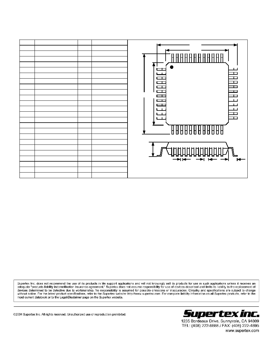
Pin Configuration
48-Lead LQFP
Pin Function
Pin Function
1 POSA/POS1A 25
DV
DD
2
2 NEGA/NEG1A 26
DGND
3 HVEN1A/POS2A
27
Out-NB2
4 HVEN2A/NEG2A
28
DV
DD
1
5 CLAMPA
29
Out-NB3
6 AV
DD
1 30
DGND
7 AGND
31
DV
DD
1
8 CLAMPB
32
Out-NA3
9 HVEN2B/NEG2B
33
DV
DD
1
10 HVEN1B/POS2B 34 Out-NA2
11 NEGB/NEG1B 35 DGND
12 POSB/POS1B 36 DV
DD
2
13 SEL
37 Out-NA1
14 AV
SS
38
N/C
15 AV
SS
39
Out-PA1
16 DV
SS
40
DV
DD
2
17 Out-PB3
41 Out-PA2
18
DGND
42 DV
DD
1
19 DV
DD
1 43
DGND
20 Out-PB2
44 Out-PA3
21 DV
DD
2 45
DV
SS
22 Out-PB1
46 V
LL
23 N/C
47 EN
24 Out-NB1
48 AV
SS
48-Lead LQFP
Top view
All dimensions are in millimeters
Doc. No. DSFP-MD1711 NR012505
7.
00
9.
00
9.
00
7.
00
1.
50
0.
22
0.
50
1.
00