MD1811
High Speed Quad MOSFET Driver
1
NR090105
Initial Release
Features
6ns rise and fall time
2 A peak output source/sink current
1.2V to 5V input CMOS compatible
5V to 12V total supply voltage
Smart Logic threshold
Low jitter design
Quad matched channels
Drives two N and two P Channel MOSFETs
Outputs can swing below ground
Low inductance quad fl at no-lead package
High-performance thermally-enhanced
Applications
Medical ultrasound imaging
Piezoelectric transducer drivers
Nondestructive evaluation
PIN diode driver
Clock driver/buffer
High speed level translator
General Description
The Supertex MD1811 is a high speed, quad MOSFET driver designed to
drive high voltage P/N-channel MOSFETs for medical ultrasound applications
and other applications requiring a high output current for a capacitive load.
The high-speed input stage of the MD1811 can operate from a 1.2 to 5.0
volt logic interface with an optimum operating input signal range of 1.8 to 3.3
volts. An adaptive threshold circuit is used to set the level translator switch
threshold to the average of the input logic 0 and logic 1 levels. The input
logic levels may be ground referenced, even though the driver is putting
out bipolar signals. The level translator uses a proprietary circuit, which
provides DC coupling together with high-speed operation.
The output stage of the MD1811 has separate power connections enabling
the output signal L and H levels to be chosen independently from the supply
voltages used for the majority of the circuit. As an example, the input logic
levels may be 0 and 1.8 volts, the control logic may be powered by +5 and
�5 volts, and the output L and H levels may be varied anywhere over the
range of �5 to +5 volts. The output stage is capable of peak currents of up
to �2 amps, depending on the supply voltages used and load capacitance
present. The OE pin serves a dual purpose. First, its logic H level is used
to compute the threshold voltage level for the channel input level translators.
Secondly, when OE is low, the outputs are disabled, with the A & C output
high and the B & D output low. This assists in properly pre-charging the AC
coupling capacitors that may be used in series in the gate drive circuit of an
external PMOS and NMOS transistor pair.
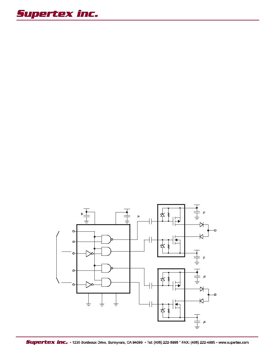
Typical Application Circuit
3.3V CMOS
Logic Inputs
OUTA
OUTB
OUTC
OUTD
+10V
0.22 F
V
DD
V
H
+10V
0.47 F
V
SS
V
L
GND
INA
INB
INC
IND
OE
+PLS1
-PLS1
ENAB
+PLS2
-PLS2
10nF
10nF
10nF
+100V
1 F
To Piezoelectric
Transducer #1
-100V
1 F
Supertex
TC6320
Supertex
TC6320
10nF
+100V
1 F
-100V
1 F
To Piezoelectric
Transducer #2
#1
#2
Supertex MD1811
2
NR090105
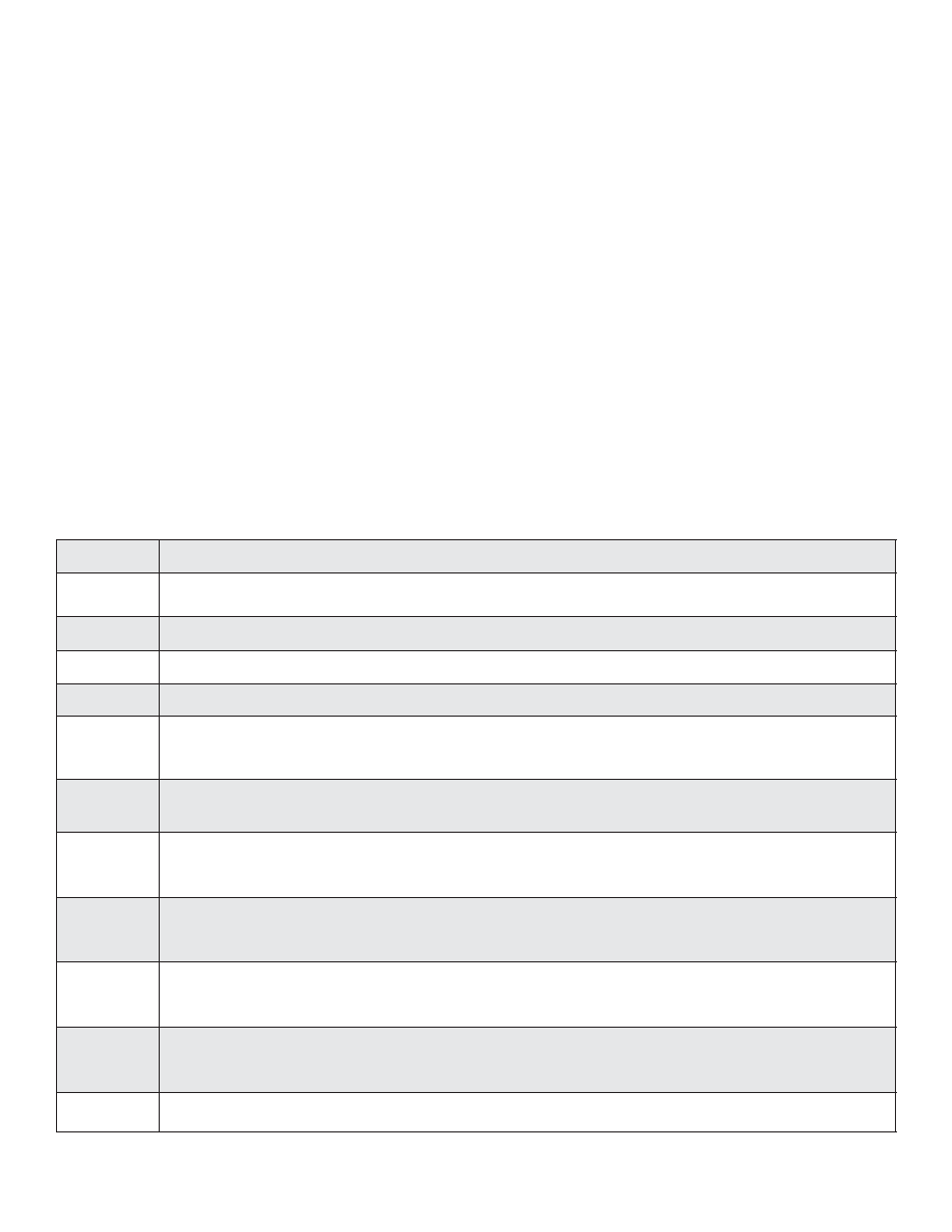
MD1811
V
DD
-V
SS
Logic supply voltage
4.5
13
V
V
SS
Low side supply voltage
-5.5
0
V
V
H
Output high supply voltage
V
SS
+2
V
DD
V
V
L
Output low supply voltage
V
SS
V
DD
-2
V
I
DDQ
V
DD
quiescent current
0.8
mA
No input transitions, OE = 1
I
HQ
V
H
quiescent current
10
�A
I
DD
V
DD
average current
8.0
mA
One channel on at 5.0Mhz, No load
I
H
V
H
average current
26
mA
V
IH
Input logic voltage high
V
OE
-0.3
5
V
For logic inputs INA, INB, INC, and IND
V
IL
Input logic voltage low
0
0.3
V
I
IH
Input logic current high
1.0
�A
I
IL
Input logic current low
1.0
�A
V
IH
OE Input logic voltage high
1.2
5
V
For logic input OE
V
IL
OE Input logic voltage low
0
0.3
V
R
IN
Input logic impedance to GND
12
20
30
K
C
IN
Logic input capacitance
5
10
pF
R
SINK
Output sink resistance
12.5
I
SINK
= 50mA
R
SOURCE
Output source resistance
12.5
I
SOURCE
= 50mA
I
SINK
Peak output sink current
2.0
A
I
SOURCE
Peak output source current
2.0
A
Outputs
(V
H
= V
DD
= 12V, V
L
= V
SS
= GND = 0V, V
OE
= 3.3V, T
J
= 25�C)
Sym.
Parameter
Min.
Typ.
Max.
Units
Conditions
Ordering Information
DEVICE
Package Options
16-Lead 4x4x0.9 QFN
MD1811
MD1811K6-G
JA
45�C/W (1oz. 4-layer 3x4inch PCB)
DC Electrical Characteristics
(V
H
= V
DD
= 12V, V
L
= V
SS
= GND = 0V, V
OE
= 3.3V, T
J
= 25�C)
Sym.
Parameter
Min.
Typ.
Max.
Units
Conditions
Product Marking Information
1
ST
Line
Device Number
1811
2
ND
Line
Year, Week Code, Lot Number
YWLL
Example: 5A88 means Lot #88 of fi rst or second week in 2005
Absolute Maximum Ratings*
V
DD
-V
SS
, Logic Supply Voltage
-0.5V to +13.5V
V
H
, Output High Supply Voltage
V
L
-0.5V to V
DD
+0.5V
V
L
, Output Low Supply Voltage
V
SS
-0.5V to V
H
+0.5V
Vss, Low Side Supply Voltage
-7V to +0.5V
Logic Input Levels
V
SS
-0.5V to V
SS
+7V
Maximum Junction Temperature
+125�C
Storage Temperature
-65�C to 150�C
Soldering Temperature
235�C
Package Power Dissipation
2.2W
Pin 1
1811
YWLL
Top View
-G indicates package is RoHS compliant (`Green')
*Absolute Maximum Ratings are those values beyond which damage to the device may occur.
Functional operation under these conditions is not implied. Continuous operation of the device
at the absolute rating level may affect device reliability. All voltages are referenced to device
ground.
3
NR090105
MD1811
AC Electrical Characteristics
(V
H
= V
DD
= 12V, V
L
= V
SS
= GND = 0V, V
OE
= 3.3V, T
J
= 25�C)
Sym.
Parameter
Min.
Typ.
Max.
Units
Conditions
t
irf
Input or OE rise & fall time
10
ns
Logic input edge speed requirement
t
PLH
Propagation delay when output
is from low to high
7
ns
C
LOAD
= 1000pF, see timing diagram
Input signal rise/fall time 2ns
t
PHL
Propagation delay when output
is from high to low
7
ns
t
POE
Propagation delay OE to output
9
ns
t
r
Output rise time
6
ns
t
f
Output fall time
6
ns
l t
r
- t
f
l
Rise and fall time matching
1.0
ns
for each channel
l
t
PLH
-t
PHL
l
Propagation low to high and
high to low matching
1.0 ns
t
dm
Propagation delay matching
�2.0
ns
Device to device delay match
Logic Truth Table
Logic Inputs
Output
OE
INA
INB
OUTA
OUTB
H
L
L
V
H
V
H
H
L
H
V
H
V
L
H
H
L
V
L
V
H
H
H
H
V
L
V
L
L
X
X
V
H
V
L
OE
INC
IND
OUTC
OUTD
H
L
L
V
H
V
H
H
L
H
V
H
V
L
H
H
L
V
L
V
H
H
H
H
V
L
V
L
L
X
X
V
H
V
L
Timing Diagram and V
TH
/ V
OE
Curve
V
OE
V
TH
0
0.5
1.0
1.5
2.0
1.0
2.0
3.0
4.0
5.0
0
0.6V
V
OE/2
0
V
1.
8 V
IN
t
PLH
1
0
%
9
0
%
5
0
%
0
V
1
2 V
5
0
%
OUT
t
PHL
t
r
9
0
%
1
0
%
t
f
V
TH
vs V
OE
4
NR090105
MD1811
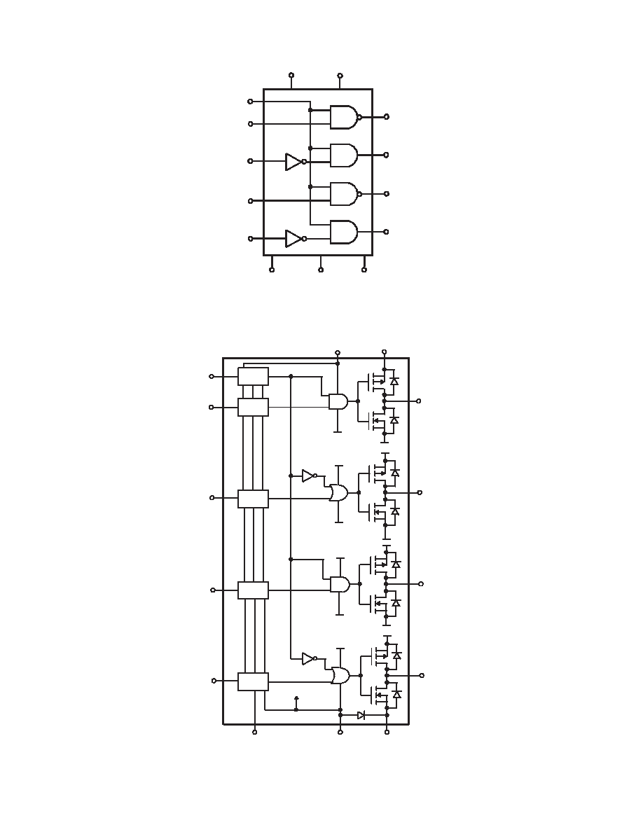
Simplifi ed Block Diagram
Detailed Block Diagram
O
E
I
N
A
I
N
B
O
U
T
A
O
U
T
B
V
D
D
V
H
I
N
C
I
N
D
O
U
T
C
O
U
T
D
G
N
D
V
S
S
V
L
MD1811
INB
Level
Shifter
V
DD
OUTC
OUTD
GND
V
L
Level
Shifter
V
H
Level
Shifter
V
L
V
SS
V
DD
V
DD
V
H
V
H
OE
INA
Level
Shifter
V
SS
Level
Shifter
V
L
OUTB
OUTA
V
DD
V
H
INC
IND
V
SS
SUB
V
SS
V
L
5
NR090105
MD1811
Application Information
For proper operation of the MD1811, low inductance bypass
capacitors should be used on the various supply pins. The GND
pin should be connected to the logic ground. The INA, INB INC,
IND, and OE pins should be connected to a logic source with a
swing of GND to V
LL
, where V
LL
is 1.2 to 5.0 volts. Good trace
practices should be followed corresponding to the desired operating
speed. The internal circuitry of the MD1811 is capable of operating
up to 100MHz, with the primary speed limitation being the loading
effects of the load capacitance. Because of this speed and the
high transient currents that result with capacitive loads, the bypass
capacitors should be as close to the chip pins as possible. Unless
the load specifi cally requires bipolar drive, the V
SS
, and V
L
pins
should have low inductance feed-through connections directly to a
ground plane. If these voltages are not zero, then they need bypass
capacitors in a manner similar to the positive power supplies. The
power connection V
DD
should have a ceramic bypass capacitor to
the ground plane with short leads and decoupling components to
prevent resonance in the power leads.
The voltages of V
H
and V
L
decide the output signal levels. These
two pins can draw fast transient currents of up to 2A, so they
should be provided with an appropriate bypass capacitor located
next to the chip pins. A ceramic capacitor of up to 1.0�F may be
appropriate, with a series ferrite bead to prevent resonance in the
power supply lead coming to the capacitor. Pay particular attention
to minimizing trace lengths, current loop area and using suffi cient
trace width to reduce inductance. Surface mount components are
highly recommended. Since the output impedance of this driver is
very low, in some cases it may be desirable to add a small series
resistance in series with the output signal to obtain better waveform
transitions at the load terminals. This will of course reduce the
output voltage slew rate at the terminals of a capacitive load.
Pay particular attention that parasitic couplings are minimized from
the output to the input signal terminals. The parasitic feedback may
cause oscillations or spurious waveform shapes on the edges of
signal transitions. Since the input operates with signals down to
1.2V even small coupled voltages may cause problems. Use of
a solid ground plane and good power and signal layout practices
will prevent this problem. Be careful that a circulating ground
return current from a capacitive load cannot react with common
inductance to cause noise voltages in the input logic circuitry.
Pin Description
V
DD
High side analog circuit, level shifter and gate drive supply voltage.
V
SS
Low side analog circuit, level shifter and gate drive supply voltage. V
SS
must be connected to the most negative
potential of voltage supplies and powered-up fi rst.
V
H
Supply voltage for P-channel output stage
V
L
Supply voltage for N-channel output stage
GND
Logic input ground reference
OE
Output-Enable logic input. When OE is high, (V
OE
+V
GND
)/2 sets the logic threshold level for inputs, When OE is low,
OUTA and OUTC are at V
H
, OUTB and OUTD are at V
L
, regardless of the inputs INA, INB, INC or IND. Keep OE
low until IC powered up
INA, INB,
INC, IND
Logic input. Controls output when OE is high. Input logic high will cause the output to swing to V
L
. Input logic low
will cause the output to swing to V
H
. Keep all logic inputs low until IC powered up.
OUTA
Output driver. Swings from V
H
to V
L
. Intended to drive the gate of an external P-channel MOSFET via a series
capacitor. When OE is low, the output is disabled. OUTA will swing to V
H
turning off the external P-channel
MOSFET.
OUTB
Output driver. Swings from V
H
to V
L
. Intended to drive the gate of an external N-channel MOSFET via a series
capacitor. When OE is low, the output is disabled. OUTB will swing to V
L
turning off the external N-channel
MOSFET.
OUTC
Output driver. Swings from V
H
to V
L
. Intended to drive the gate of an external P-channel MOSFET via a series
capacitor. When OE is low, the output is disabled. OUTC will swing to V
H
turning off the external P-channel
MOSFET.
OUTD
Output driver. Swings from V
H
to V
L
. Intended to drive the gate of an external N-channel MOSFET via a series
capacitor. When OE is low, the output is disabled. OUTD will swing to V
L
turning off the external N-channel
MOSFET.
Substrate
The IC substrate is internally connected to the thermal pad. Thermal Pad and V
SS
must be connected externally.
6
Doc.# DSFP - MD1811 NR090105
MD1811
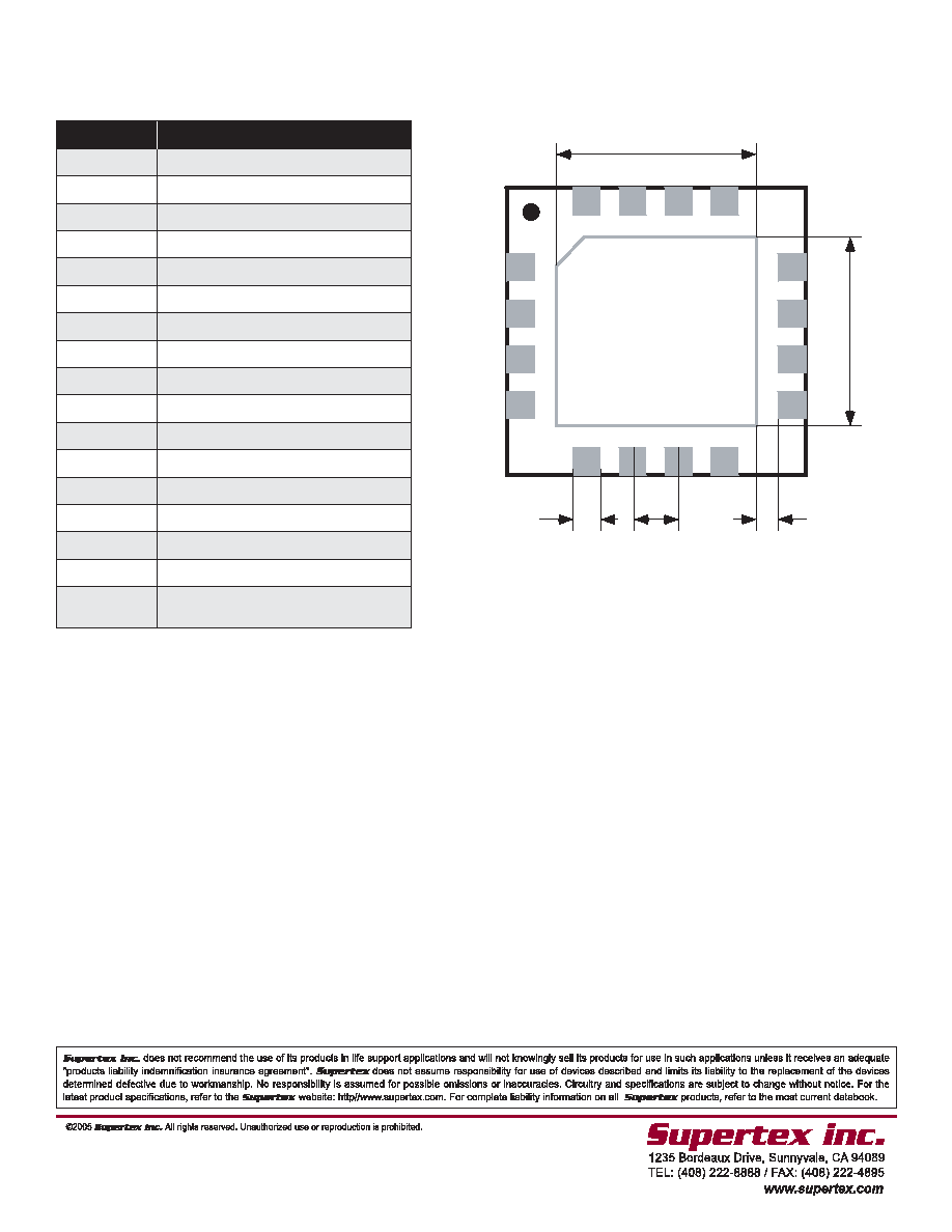
Pin Confi guration
Pin #
Function
1
INB
2
V
L
3
GND
4
V
L
5
INC
6
IND
7
V
SS
8
OUTD
9
OUTC
10
V
H
11
V
H
12
OUTB
13
OUTA
14
V
DD
15
INA
16
OE
Note
Thermal Pad, and Pin #7 (V
SS
), must be
connected externally
QFN-16
4x4x0.9
1
9
16
(Top View, mm)
13
0.325
0.65
2.64
2.64
0.28
4
12
5
8