Supertex inc.
Supertex inc.
∑
1235 Bordeaux Drive, Sunnyvale, CA 94089
∑
Tel: (408) 222-8888
∑
FAX: (408) 222-4895
∑
www.supertex.com
1
NR031706
MD1812
Initial Release
Features
6ns rise and fall time
2A peak output source/sink current
1.2V to 5V input CMOS compatible
±5V to ±12V supply voltage operation
Smart Logic threshold
Low jitter design
Quad matched channels
Drives two N and two P-channel MOSFETs
Outputs can swing below ground
Built-in level translator for negative gate bias
User-defi ned damping for return-to-zero application
Low inductance quad fl at no-lead package
Thermally-enhanced package
Applications
Ultrasound PN code transmitter
Medical ultrasound imaging
Piezoelectric transducer drivers
Nondestructive evaluation
High speed level translator
High voltage bipolar pulser
General Description
The Supertex MD1812 is a high-speed quad MOSFET driver. It is
designed to drive two N and two P-channel high voltage DMOS FETs for
medical ultrasound applications but may be used in any application that
needs a high output current for a capacitive load. The input stage of the
MD1812 is a high-speed level translator that is able to operate from logic
input signals of 1.2 to 5.0 volt amplitude. An adaptive threshold circuit
is used to set the level translator threshold to the average of the input
logic 0 and logic 1 levels. The level translator uses a proprietary circuit,
which provides DC coupling together with high-speed operation. The
output stage of the MD1812 has separate power connections enabling
the output signal L and H levels to be chosen independently from the
driver supply voltages.
As an example, the input logic levels may be 0V and 1.8V, the control
logic may be powered by +5V and ≠5V, and the output L and H levels
may be varied anywhere over the range of ≠5V to +5V. The output stage
is capable of peak currents of up to ±2 amps, depending on the supply
voltages used and load capacitance. The OE pin serves a dual purpose.
First, its logic H level is used to compute the threshold voltage level for the
channel input level translators. Secondly, when OE is low, the outputs are
disabled, with the A and C outputs high and the B and D outputs low. This
assists in properly pre-charging the coupling capacitors that may be used
in series in the gate drive circuit of an external PMOS and NMOS. A built-
in level shifter provides P-MOS gate negative bias drive. This enables the
user-defi ned damping control to generate return-to-zero bipolar output
pulses.
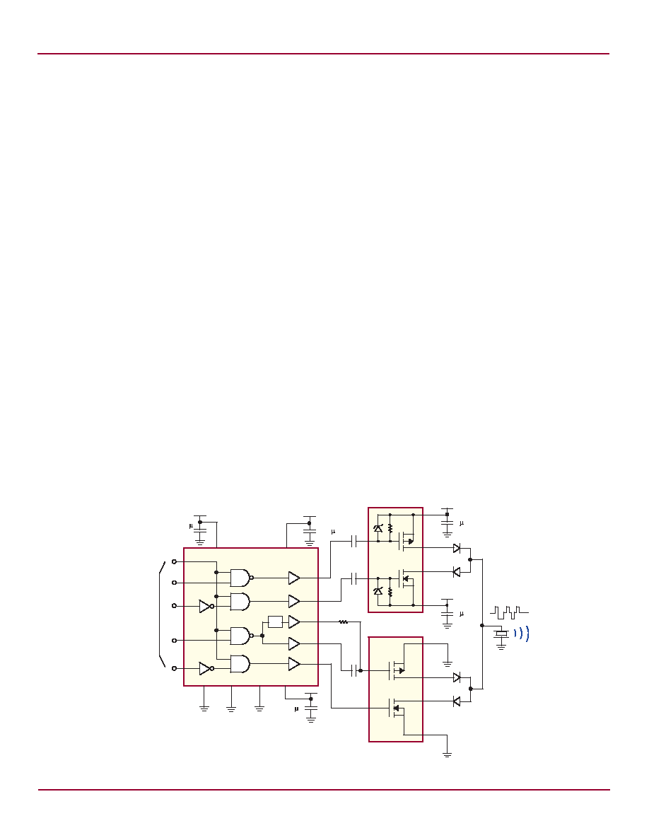
Typical Application Circuit
High Speed Quad MOSFET Driver
3.3V CMOS
Logic Inputs
10nF
10nF
10nF
+100V
1 F
OUT
A
OUT
B
-100V
1 F
OUT
C
OUT
D
+10V
0.22 F
V
DD
V
H
+10V
0.47 F
V
SS
V
L
V
NEG
GND
IN
A
IN
B
IN
C
IN
D
OE
-10V
0.47 F
LT
2K
OUT
G
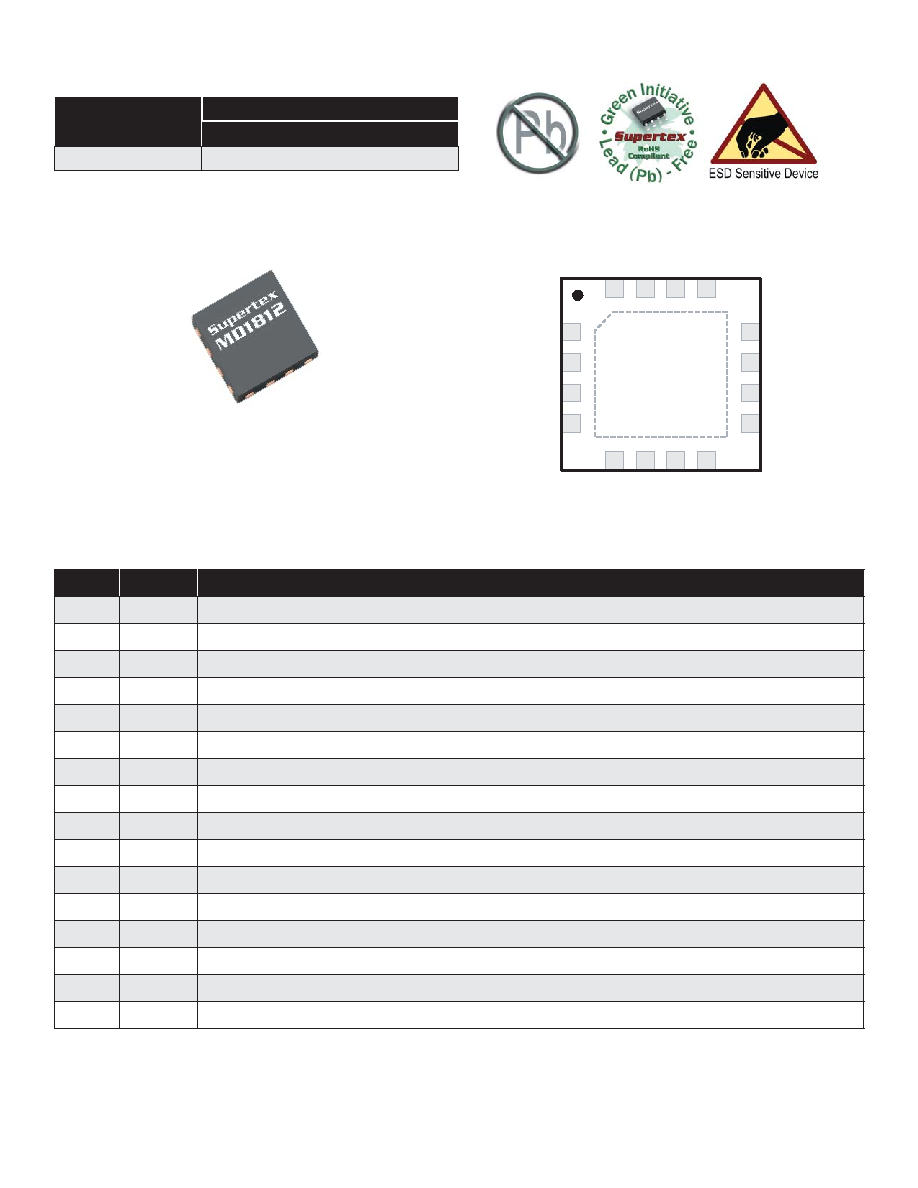
Supertex
MD1812
Supertex
TC2320
Supertex
TC6320
16
15
1
5
6
3
7
2
4
8
9
10
12
13
11
14
2
NR031706
MD1812
Device
Package Option
16-lead 4x4x0.9 QFN
MD1812
MD1812K6-G
-G indicates package is RoHS compliant (`Green')
1
9
16
13
4
12
5
8
Top View
MD1812
Note: Thermal pad and pin #4, V
NEG
must be connected externally.
Pin #
Function
Description
1
IN
B
Logic input. Controls OUT
B
when OE is high.
.
2
V
L
Supply voltage for N-channel output stage.
3
GND
Device ground.
4
V
NEG
Supply voltage the auxiliary gate drive.
5
IN
C
Logic input. Controls OUT
C
when OE is high.
6
IN
D
Logic input. Controls OUT
D
when OE is high.
7
V
SS
Supply voltage for low-side analog, level shifter, and gate drive circuit.
8
OUT
D
Output driver.
9
OUT
C
Output driver.
10
OUT
G
Auxiliary output driver.
11
V
H
Supply voltage for P-channel output stage
12
OUT
B
Output driver.
13
OUT
A
Output driver.
14
V
DD
Supply voltage for high-side analog, level shifter, and gate drive circuit.
15
IN
A
Logic input. Controls OUT
A
when OE is high.
16
OE
Output enable logic input.
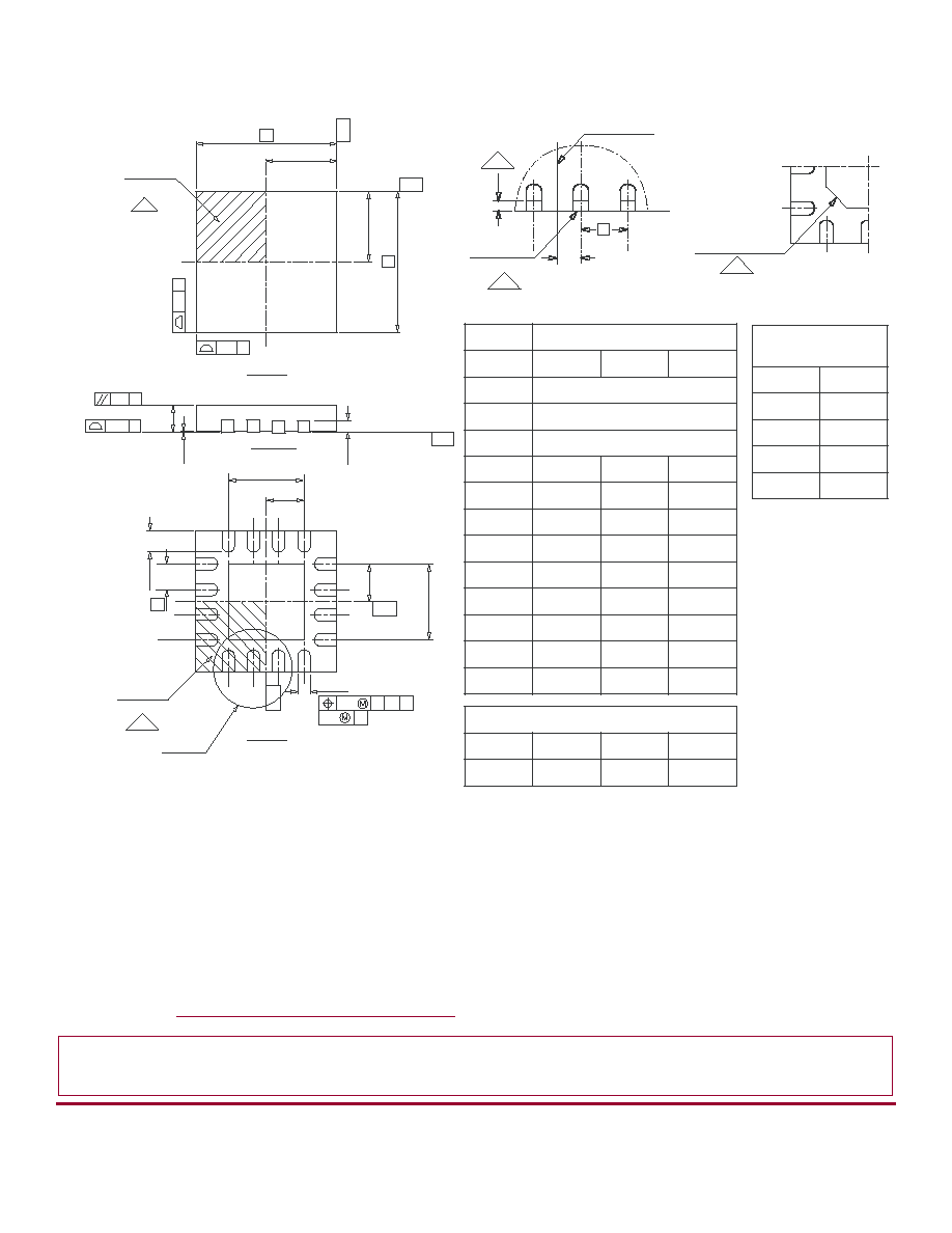
16-Lead QFN (K6) Package
Pin Description
16-Lead QFN (K6) Pin Confi guration
3
NR031706
MD1812
Symbol
Parameter
Min
Typ
Max
Units
Conditions
V
DD
- V
SS
Logic supply voltage
4.5
-
13
V
---
V
SS
Low side supply voltage
-5.5
-
0
V
---
V
H
Output high supply voltage
V
SS
+2
-
V
DD
V
---
V
L
Output low supply voltage
V
SS
-
V
DD
-2
V
---
V
NEG
Negative supply voltage
-13
-
V
SS
-2
V
May connect to V
SS
if OUT
G
not used
I
DDQ
V
DD
quiescent current
-
1.5
-
mA
No input transitions, OE = 1
I
HQ
V
H
quiescent current
-
-
10
µA
I
NEGQ
V
NEG
quiescent current
-
-
10
µA
I
DD
V
DD
average current
-
7.0
-
mA
One channel on at 5.0Mhz, No load
I
H
V
H
average current
-
22
-
mA
I
NEG
V
NEG
average current
-
1.5
-
mA
V
IH
Input logic voltage high
V
OE
-0.3
-
5
V
For logic inputs IN
A
, IN
B
, IN
C
, and IN
D
V
IL
Input logic voltage low
0
-
0.3
V
I
IH
Input logic current high
-
-
1.0
µA
I
IL
Input logic current low
-
-
1.0
µA
V
IH
OE Input logic voltage high
1.2
-
5
V
For logic input OE
V
IL
OE Input logic voltage low
0
-
0.3
V
R
IN
Input logic impedance to GND
12
20
30
K
C
IN
Logic input capacitance
-
5
10
pF
---
Absolute Maximum Ratings
Parameter
Value
V
DD
-V
SS
, Logic Supply Voltage
-0.5V to +13.5V
V
H
, Output High Supply Voltage
V
L
-0.5V to V
DD
+0.5V
V
L
, Output Low Supply Voltage
V
SS
-0.5V to V
H
+0.5V
Vss, Low Side Supply Voltage
-7V to +0.5V
V
NEG
-V
SS
, Negative Supply Voltage
V
SS
-13.5V to V
SS
+0.5V
Logic Input Levels
V
SS
-0.5V to V
SS
+7V
Maximum Junction Temperature
+125∞C
Storage Temperature
-65∞C to 150∞C
Soldering Temperature
235∞C
Package Power Dissipation
2.2W
Absolute Maximum Ratings are those values beyond which damage to the
device may occur. Functional operation under these conditions is not implied.
Continuous operation of the device at the absolute rating level may affect
device reliability. All voltages are referenced to device ground.
DC Electrical Characteristics
(V
H
= V
DD
= 12V, V
L
= V
SS
= GND = 0V, V
NEG
= -12V, V
OE
= 3.3V, T
J
= 25
O
C)
4
NR031706
MD1812
R
SINK
Output sink resistance
-
-
12.5
I
SINK
= 50mA
R
SOURCE
Output source resistance
-
-
12.5
I
SOURCE
= 50mA
I
SINK
Peak output sink current
-
2.0
-
A
---
I
SOURCE
Peak output source current
-
2.0
-
A
---
Symbol
Parameter
Min
Typ
Max
Units
Conditions
Symbol
Parameter
Min
Typ
Max
Units
Conditions
t
irf
Input or OE rise & fall time
-
-
10
ns
Logic input edge speed requirement
t
PLH
Propagation delay when output is
from low to high
-
7
-
ns
C
LOAD
= 1000pF, see timing diagram
Input signal rise/fall time 2ns
t
PHL
Propagation delay when output is
from high to low
-
7
-
ns
t
POE
Propagation delay OE to output
-
9
-
ns
t
PCG
Propagation delay IN
C
to OUT
G
-
28
-
ns
t
r
Output rise time
-
6
-
ns
t
f
Output fall time
-
6
-
ns
l t
r
- t
f
l
Rise and fall time matching
-
1.0
-
ns
for each channel
l t
PLH
-t
PHL
l
Propagation low to high and high
to low matching
-
1.0
-
ns
t
dm
Propagation delay matching
-
±2.0
-
ns
Device to device delay match
Logic Inputs
Output
OE
IN
A
IN
B
OUT
A
OUT
B
H
L
L
V
H
V
H
H
L
H
V
H
V
L
H
H
L
V
L
V
H
H
H
H
V
L
V
L
L
X
X
V
H
V
L
OE
IN
C
IN
D
OUT
C
OUT
G
OUT
D
H
L
L
V
H
V
SS
V
H
H
L
H
V
H
V
SS
V
L
H
H
L
V
L
V
NEG
V
H
H
H
H
V
L
V
NEG
V
L
L
X
X
V
H
V
SS
V
L
Outputs
(V
H
= V
DD
= 12V, V
L
= V
SS
= GND = 0V, V
NEG
= -12V, V
OE
= 3.3V, T
J
= 25
O
C)
AC Electrical Characteristics
(V
H
= V
DD
= 12V, V
L
= V
SS
= GND = 0V, V
NEG
= -12V, V
OE
= 3.3V, T
J
= 25
O
C)
Logic Truth Table

5
NR031706
MD1812
Application Information
For proper operation of the MD1812, low inductance bypass
capacitors should be used on the various supply pins. The GND pin
should be connected to the logic ground. The IN
A
, IN
B
, IN
C
, IN
D
and
OE pins should be connected to a logic source with a swing of GND
to V
CC
, where V
CC
is 1.2 to 5.0 volts. When input logic(s) is high,
output(s) will swing to V
L
, and when input(s) logic is low, output(s) will
swing to V
H
. All inputs must be kept low until the device is powered
up. Good trace practices should be followed corresponding to the
desired operating speed. The internal circuitry of the MD1812 is
capable of operating up to 100MHz, with the primary speed limitation
being the loading effects of the load capacitance. Because of this
speed and the high transient currents that result with capacitive
loads, the bypass capacitors should be as close to the chip pins as
possible. Unless the load specifi cally requires bipolar drive, the V
SS
and V
L
pins should have low inductance feed-through connections
directly to a ground plane. If these voltages are not zero, then they
need bypass capacitors in a manner similar to the positive power
supplies. The power connection V
DD
should have a ceramic bypass
capacitor to the ground plane, with short leads and decoupling
components to prevent resonance in the power leads.
Output drivers, OUT
A
and OUT
C
, drive the gate of an external P-
channel MOSFET, while output drivers OUT
B
and OUT
D
drive the
gate of an external N-channel MOSFET, and they all swing from
V
H
to V
L
. The auxiliary output drive, OUT
G
, swings from V
SS
to V
NEG
,
and drives the gate of an external P-channel MOSFET via a 2K
series resistor.
The voltages of V
H
and V
L
decide the output signal levels. These
two pins can draw fast transient currents of up to 2A, so they
should be provided with an appropriate bypass capacitor located
next to the chip pins. A ceramic capacitor of up to 1.0µF may be
appropriate, with a series ferrite bead to prevent resonance in the
power supply lead coming to the capacitor. Pay particular attention
to minimizing trace lengths, current loop area, and using suffi cient
trace width to reduce inductance. Surface mount components are
highly recommended. Since the output impedance of this driver is
very low, in some cases it may be desirable to add a small series
resistance in series with the output signal to obtain better waveform
transitions at the load terminals. This will reduce the output voltage
slew rate at the terminals of a capacitive load.
The OE pin sets the threshold level of logic for inputs (V
OE
+ V
GND
)
/ 2. When OE is low, OUT
A
and OUT
C
are at V
H
. OUT
B
and OUT
D
are at V
L
. Auxiliary output OUT
G
, is at V
SS
, regardless of the inputs
IN
A
or IN
B
.
Pay particular attention that parasitic couplings are minimized from
the output to the input signal terminals. The parasitic feedback may
cause oscillations or spurious waveform shapes on the edges of
signal transitions. Since the input operates with signals down to
1.2V, even small coupled voltages may cause problems. Use of
a solid ground plane and good power and signal layout practices
will prevent this problem. Be careful that a circulating ground
return current from a capacitive load cannot react with common
inductance to cause noise voltages in the input logic circuitry. Best
timing performance is obtained for OUT
C
when the voltage of (V
SS
-
V
NEG
) = (V
H
-V
L
).
Supertex inc.
1235 Bordeaux Drive, Sunnyvale, CA 94089
TEL: (408) 222-8888 / FAX: (408) 222-4895
www.supertex.com
©2006 Supertex inc. All rights reserved. Unauthorized use or reproduction is prohibited.
Supertex inc.
does not recommend the use of its products in life support applications, and will not knowingly sell its products for use in such applications, unless it receives an adequate
"product liability indemnification insurance agreement". Supertex does not assume responsibility for use of devices described and limits its liability to the replacement of the devices
determined defective due to workmanship. No responsibility is assumed for possible omissions or inaccuracies. Circuitry and specifications are subject to change without notice. For the latest
product specifications, refer to the Supertex website: http//www.supertex.com.
6
Doc.# DSFP - MD1812
NR031706
MD1812
16-Lead QFN Package Outline (K6)
-C-
A3
A1
SIDE VIEW
PLANE
A
ccc C
0.08 C
NX
SEATING
D
D/2
INDEX AREA
E
a
aa
C
aaa C
TOP VIEW
2x
2x
4
(D/2 xE/2)
2
/
E
-B-
A
-
-
X
Nl
e
NXb
D2/2
D2
/
2
E2
1
E2
bbb
C A B
ddd
C
-B-
A
--
N
N-1
BTM VIEW
(D/2 xE/2)
INDEX AREA
4
SEE
DETAIL B
e
Terminal Tip
5
Datum A or B
4
l1
e/2
1
N
N-1
&
m
r
o
F
f
o
e
c
n
a
r
e
l
o
T
n
o
i
t
i
s
o
P
a
a
a
5
1
.
0
b
b
b
0
1
.
0
c
c
c
0
1
.
0
d
d
d
5
0
.
0
e
u
s
s
I
A
s
n
o
i
s
n
e
m
i
D
D
I
m
o
t
t
o
B
A
A
B
B
C
C
D
D
4
4
3
.
4
4
3
.
1
8
1
.
1
8
1
.
Notes:
1. Dimensioning and tolerancing conform to ASME Y14.5m - 1994.
2. All dimensions are in millimeters, all angles are in degrees (
O
).
3. The terminal #1 identifier and terminal numbering convention shall conform to JEDEC publication 95, SPP-002. Details of terminal #1 identifier are
optional, but must be located within the zone indicated. The terminal #1identifier may be either a mold or marked feature.
4. Depending on the method of lead termination at the edge of the package, pull back (L1) may be present. L minus L1 to be equal to or greater than
0.33mm.
5. Dimension B applies to metallized terminal and is measured between 0.15mm and 0.30mm from the terminal tip. If the terminal has the optional radius
on the other end of the terminal, the dimension B should not be measured in that radius area.
l
o
b
m
y
S
s
n
o
i
s
n
e
m
i
D
t
h
g
i
e
H
n
i
M
m
o
N
x
a
M
C
S
B
D
0
.
4
C
S
B
E
0
.
4
e
5
6
.
0
2
D
0
.
2
5
1
.
2
5
2
.
2
2
E
0
.
2
5
1
.
2
5
2
.
2
b
5
2
.
0
0
3
.
0
5
3
.
0
l
5
4
.
0
5
5
.
0
5
6
.
0
A
0
8
.
0
0
9
.
0
0
.
1
1
A
0
0
.
0
2
0
.
0
5
0
.
0
3
A
-
-
-
f
e
r
0
2
.
0
-
-
-
1
L
3
0
.
0
-
-
-
5
1
.
0
e
u
s
s
I
A
Chamfer/Radius
4
(The package drawing(s) in this data sheet may not refl ect the most current specifi cations. For the latest package outline
information go to
http://www.supertex.com/packaging.html
.)