 | –≠–ª–µ–∫—Ç—Ä–æ–Ω–Ω—ã–π –∫–æ–º–ø–æ–Ω–µ–Ω—Ç: PS11NG | –°–∫–∞—á–∞—Ç—å:  PDF PDF  ZIP ZIP |
PS10/PS11
1
Quad Power Sequencing Controller
Features
Sequencing of Four or More* Supplies, ICs, or Sub-
systems
Independently Programmable Delays Between Open
Drain PWRGD Flags (5ms to 200ms)
±10V to ±90V Operation
Tracking in Combination with Schottky Diodes
Input Supervisors Including:
o
UV/OV Lock Out/Enable
o
Power-On-Reset (POR)
Low Power Consumption, 0.4mA Supply Current
Small SO-14 Package
*By Daisy-Chaining PS10/11's
Applications
Power Supply Sequencing
-48V Telecom and Networking Distributed Systems
-24V Cellular and Fixed Wireless Systems
-24V PBX Systems
+48V Storage Systems
FPGA, Microprocessor Tracking
Industrial/Embedded System Timing/Sequencing
High Voltage MEMs Driver's Supply Sequencing
High Voltage Display Driver's Supply Sequencing
Description
Many of today's high performance FPGA's, Microproces-
sors, DSP and industrial/embedded subsystems require
sequencing of the input power. Historically this has been
accomplished: i) discretely using comparators, references
& RC circuits; ii) using expensive programmable control-
lers; or iii) with low voltage sequencers requiring resistor
drop downs and several high voltage optocoupler or level
shift components.
The PS10/11 saves board space, improves accuracy,
eliminates optocouplers or level shifts and reduces overall
component count by combining four timers, programmable
input UV/OV supervisors, a programmable POR and four
90V open drain outputs. A high reliability, high voltage,
junction isolated process allows the PS10/11 to be con-
nected directly across the high voltage input rails.
The power-on-reset interval (POR) may be programmed
by a capacitor on Cramp. To sequence additional sys-
tems, PS10/11 may be daisy chained together. If at any
time the input supply falls outside the UV/OV detector
range the PWRGD outputs will immediately become IN-
ACTIVE. Down sequencing may be accomplished with
additional components (see page 11).
The PS10/PS11 is available in a space saving SO-14
package.
Supertex Inc. does not recommend the use of its products in life support applications and will not knowingly sell its products for use in such applications unless it receives an adequate
"products liability indemnification insurance agreement." Supertex does not assume responsibility for use of devices described and limits its liability to the replacement of devices deter-
mined to be defective due to workmanship. No responsibility is assumed for possible omissions or inaccuracies. Circuitry and specifications are subject to change without notice. For the
latest product specifications, refer to the Supertex website: http://www.supertex.com. For complete liability information on all Supertex products, refer to the most current databook or to the
Legal/Disclaimer page on the Supertex website.
Initial Release
PS10 - Active High
PS11 - Active Low
04/07/03
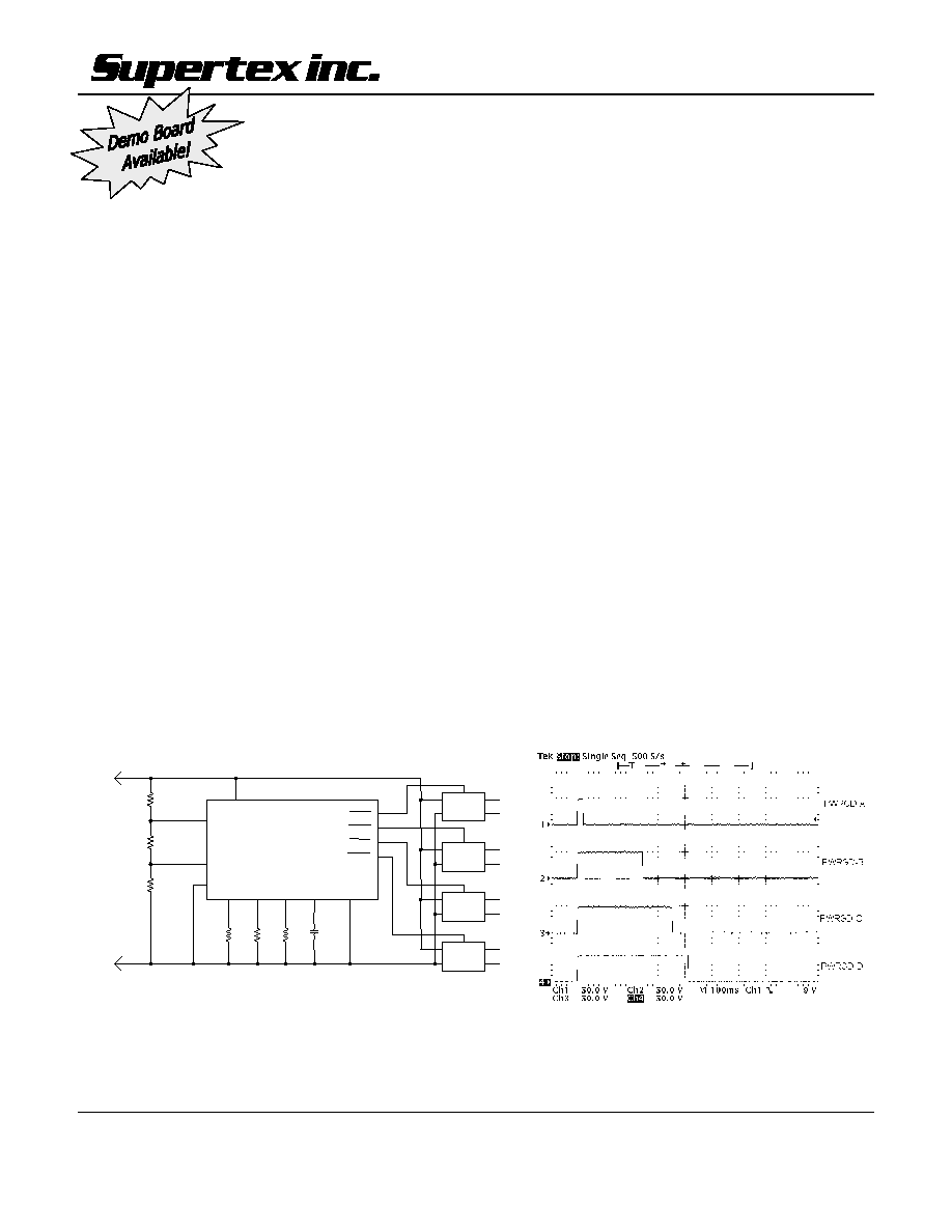
Relative to Negative Rail
TD
10
DC/DC
CONVERTER
COM
PWRGD-D / PWRGD-D
Notes:
1. Under Voltage Shutdown (UV) set to 35V.
2. Over Voltage Shutdown (OV) to 65V.
13
PWRGD-C / PWRGD-C
/EN
12
PWRGD-B / PWRGD-B
DC/DC
CONVERTER
11
PWRGD-A / PWRGD-A
/EN
RAMP
PS10/PS11
DC/DC
CONVERTER
7
V
5
COM
+12V
/EN
/EN
6
+5V
IN
V
14
TADJ
UV
487K
GND or +48V
1
+3.3V
OV
2
10nF
TB
6.81K
3
RTD
9.76K
DC/DC
CONVERTER
+2.5V
-48V or GND
RTC
4
COM
RTB
EE
TC
8
COM
Typical Application Circuit/Waveform
(49.9k pull-up on PS11 PWRGD pins)
PS10/PS11
2
*
Absolute Maximum Ratings are those values beyond which damage to the device may
occur. Functional operation under these conditions is not implied. Continuous operation of
the device at the absolute rating level may affect device reliability. All voltages are refer-
enced to device ground.
Ordering Information
Package Options
Active State of Power
Good Flags
14 Pin SOIC
High PS10NG
Low PS11NG
Absolute Maximum Ratings*
V
EE
referenced to V
IN
pin
+0.3V to -100V
V
PWRGD
referenced to V
EE
voltage
-0.3V to +100V
V
UV
and V
OV
referenced to V
EE
Voltage
-0.3V to 12V
Operating Ambient Temperature
-40∞C to +85∞C
Operating Junction Temperature
-40∞C to +125∞C
Storage Temperature Range
-65∞ to +150∞C
Electrical Characteristics
(-10V ∑ V
IN
∑ -90V, T
A
= 25∞C unless otherwise specified)
Symbol Parameter Min
Typ
Max
Units
Conditions
Supply
(Referenced to V
IN
pin)
V
EE
Supply
Voltage
-90 -10 V
I
EE
Supply
Current
400
450
µ
A
V
EE
= -48V
OV and UV Control
(Referenced to V
EE
pin)
V
UVH
UV High Threshold
1.20
1.26
1.32
V
Low to High Transition
V
UVL
UV Low Threshold
1.10
1.16
1.22
V
High to Low Transition
V
UVHY
UV
Hysteresis
100 mV
I
UV
UV Input Current
1.0
nA
V
UV
= V
EE
+ 1.9V
V
OVH
OV High Threshold
1.20
1.26
1.32
V
Low to High Transition
V
OVL
OV Low Threshold
1.10
1.16
1.22
V
High to Low Transition
V
OVHY
OV
Hysteresis
100 mV
I
OV
OV Input Current
1.0
nA
V
UV
= V
EE
+ 1.9V
Power Good Timing
(Test Conditions: C
RAMP
= 10nF, V
UV
= V
EE
+ 1.9V, V
OV
= V
EE
+ 0.5V)
I
RAMP
Ramp Pin Output Current
10
µ
A
V
TADJ
= 0V
t
PWRGD-A
Time from UV High to PWRGD-A
8.8
ms
V
EE
= -48V, C
RAMP
= 10nF,
see Typical Application Cir-
cuit
t
PWRGD-B
Maximum time from PWRGD-A to PWRGD-B
150
200*
250
ms
RTB = 120k
t
PWRGD-B
Minimum time from PWRGD-A to PWRGD-B
3.0
5.0*
8.0
ms
RTB = 3k
t
PWRGD-C
Maximum time from PWRGD-B to PWRGD-C
150
200*
250
ms
RTC = 120k
t
PWRGD-C
Minimum time from PWRGD-B to PWRGD-C
3.0
5.0*
8.0
ms
RTC = 3k
t
PWRGD-D
Maximum time from PWRGD-C to PWRGD-D
150
200*
250
ms
RTD = 120k
t
PWRGD-D
Minimum time from PWRGD-C to PWRGD-D
3.0
5.0*
8.0
ms
RTD = 3k
*Note: Variations will track. For example if t
PWRGD-A
is 250ms then so will be
t
PWRGD-B/C/D.
Contact factory for tighter tolerance version.
Power Good Outputs
(Test Conditions: V
UV
= V
EE
+ 1.9V, V
OV
= V
EE
+ 0.5V)
V
PWRGD-x(hi)
Power Good Pin Breakdown Voltage
90
V
PWRGD-x = HI Z
V
PWRGD-x(lo)
Power Good Pin Output Low Voltage
0.5
0.8
V
I
PWRGD
= 1mA, PWRGD-x = LOW
I
PWRGD-x(lk)
Maximum Leakage Current
<1.0
10
µ
A
V
PWRGD
= 90V, PWRGD-x = HI Z
PS10/PS11
3
PWRGD Logic
Model Condition PWRGD-A/B/C/D
INACTIVE (not ready)
0 V
EE
PS10
ACTIVE (Ready)
1 HI
Z
INACTIVE (not ready)
1 HI
Z
PS11
ACTIVE (Ready)
0 V
EE
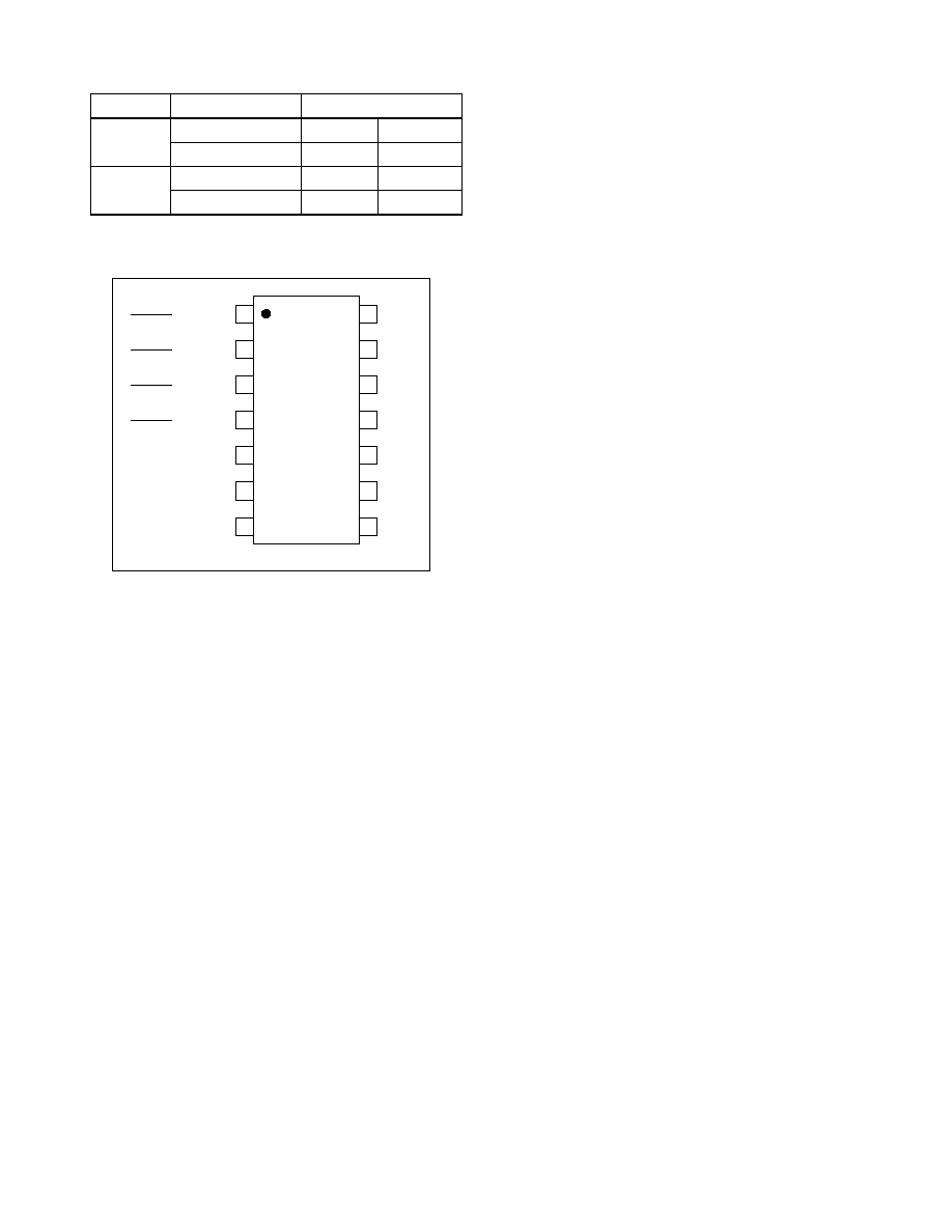
Pinout
PWRGD-B (PS11)
7
TB
PWRGD-A (PS10)
12
Top View
13
IN
PWRGD-A (PS11)
14
PWRGD-D (PS10)
9
PWRGD-D (PS11)
8
EE
OV
11
UV
10
V
PWRGD-C (PS10)
TADJ
1
NC
RAMP
2
TC
PWRGD-C (PS11)
3
5
TD
PWRGD-B (PS10)
4
6
V
Pin Description
PWRGD-D* ≠ This open drain Power Good Output Pin is
held inactive on initial power application and goes active a
programmed time delay after PWRGD-C goes active.
PWRGD-C* ≠ This open drain Power Good Output Pin is
held inactive on initial power application and goes active a
programmed time delay after PWRGD-B goes active.
PWRGD-B* ≠ This open drain Power Good Output Pin is
held inactive on initial power application and goes active a
programmed time delay after PWRGD-A goes active.
PWRGD-A* ≠ This open drain Power Good Output Pin is
held inactive on initial power application and goes active one
POR delay after the UV pin goes above its High threshold
(provided V
IN
stays within the UV/OV window during this
period).
To function as an indicator a pullup resistor must be con-
nected from this pin to a voltage rail no more than 90V from
V
EE
.
OV ≠ This Over Voltage (OV) sense pin, when raised above
its high threshold will immediately cause the Power Good
Outputs to be pulled low. These outputs will remain low until
the voltage on this pin falls below the low threshold limit,
initiating a new start-up cycle.
UV ≠ This Under Voltage (UV) sense pin, when lowered
below its low threshold will immediately cause the Power
Good Outputs to be pulled low. These outputs will remain
low until the voltage on this pin rises above the low thresh-
old limit, initiating a new start-up cycle.
V
EE
- This pin is the negative terminal of the power supply
input to the circuit.
V
IN
≠ This pin is the positive terminal of the power supply
input to the circuit and can withstand 90V with respect to
V
EE
.
TD ≠ The resistor connected from this pin to V
EE
pin sets the
time delay from PWRGD-C going active to PWRGD-D going
active.
TC ≠ The resistor connected from this pin to V
EE
pin sets the
time delay from PWRGD-B going active to PWRGD-C going
active.
TB ≠ The resistor connected from this pin to V
EE
pin sets the
time delay from PWRGD-A going active to PWRGD-B going
active.
RAMP ≠ This pin provides a current output so that a timing
ramp is generated when a capacitor is connected. This tim-
ing Ramp is used to program POR and the time from satis-
faction of the UV/OV supervisors to PWRGD-A.
TADJ≠ A voltage source (0-50mV) connected to this pin
with respect to V
EE
allows adjustment of the PWRGD-A time
delay. This allows simple interface connectivity with a
µ
C
D/A converter for adjustable timing. Normally this pin is tied
to V
EE
.
PS10/PS11
4
Functional Block Diagram
Vbg
IN
PWRGD-B
+
-
TADJ
+
UVLO
TD
Programmable
Timer
V
Regulator
& POR
-
10uA
Vint
UV
EE
+
+
Logic
Vint
RAMP
PWRGD-A
-
TC
OV
-
5k
TB
Band Gap
Reference
PWRGD-D
PWRGD-C
V
Vint - 1.2V
Functional Description
The PS10/PS11 are designed to sequence up to 4 power
supply modules, ICs or subsystems when the backplane
voltage is within the programmed Under-voltage and Over-
voltage limits. The power good open drain outputs are
sequentially enabled starting from PWRGD-A to PWRGD-
D. The time delay between power goods is programmable
up to 200ms simply by changing the value(s) of RTB,
RTC, and RTD. The initial time between satisfaction of the
UV/OV supervisors & PWRGD-A can be programmed with
Cramp.
Description of Operation
During the initial power application, the Power Good pins
are held low (rising with V
IN
) for PS10 and high for the
PS11. Once the internal under voltage lock out has been
satisfied, the circuit checks the input supply under voltage
(UV) and over voltage (OV) sense circuits to ensure that
the input voltage is within programmed limits. These limits
are determined by the selected values for R1, R2, and R3,
which form a voltage divider.
At the same time, a 10
µ
A current source is enabled,
charging the external capacitor connected to the ramp pin.
The rise time of the ramp pin is determined by the value of
the capacitor (10
µ
A/Cramp). When the ramp voltage
reaches 8.8V, the PWRGD-A pin will change into an active
state. PWRGD-B will change into an active state after a
programmed time delay from PWRGD-A inactive to active
transition. PWRGD-C will change into an active state after
a programmed time delay from PWRGD-B inactive to ac-
tive transition. PWRGD-D will change into an active state
after a programmed time delay from PWRGD-C inactive to
active transition.
The controller continuously monitors the UV and OV pins
as long as the internal UVLO and POR circuits are satis-
fied. At any time during the start up cycle or thereafter,
crossing the UV low and OV high limits will cause an im-
mediate discharge on Cramp and reset on the power good
pins. When the input voltage returns to a value within the
programmed UV and OV limits, a new start up sequence
will initiate immediately.
Programming the Under and Over Voltage Limits
The UV and OV pins are connected to comparators with
nominal 1.21V thresholds and 100mV of hysteresis (1.21V
±
50mV). They are used to detect under voltage and over
voltage conditions at the input to the circuit. Whenever the
OV pin rises above its high threshold (1.26V) or the UV pin
falls below its low threshold (1.16V), the PWRGD outputs
immediately deactivate.
Calculations can be based on either the desired input volt-
age operating limits or the input voltage shutdown limits. In
the following equations the shutdown limits are assumed.
The undervoltage and overvoltage shut down thresholds
can be programmed by means of the three resistor divider
formed by R1, R2 and R3. Since the input currents on the
UV and OV pins are negligible the resistor values may be
calculated as follows:
UV
OFF
= V
UVL
= 1.16 = (V
EEUV(off)
) x (R2+R3)/(R1+R2+R3)
OV
OFF
= V
OVL
= 1.26 = (V
EEOV(off)
) x R3/(R1+R2+R3)

PS10/PS11
5
Where (V
EEUV(off)
) and (V
EEOV(off)
) relative to V
EE
are Under and
Over Voltage Shut Down Threshold points.
If we select a divider current of 100
µ
A at a nominal oper-
ating input voltage of 50 Volts, then
R1+R2+R3 = 50V/100
µ
A = 500k
From the second equation, for an OV shut down threshold
of 65V, the value of R3 may be calculated.
OV
OFF
= 1.26 = (65xR3)/500k
R3 = (1.26x 500k)/65 = 9.69k
The closest 1% value is 9.76k
.
From the first equation, for a UV shut down threshold of
35V, the value of R2 can be calculated.
UV
OFF
= 1.16 = 35 x (R2+R3)/ 500k
R2 = ((1.16 x 500k)/35) ≠ 9.76k = 6.81k
6.81k
is a standard 1% value
Then
R1 = 500k ≠ R2 ≠ R3 = 483
.
487K
, is a standard 1% value.
From the calculated resistor values the OV and UV start
up threshold voltages can be calculated as follows:
UV
ON
= V
UVH
= 1.26 = (V
EEUV(on)
) x (R2+R3)/(R1+R2+R3)
OV
ON
= V
OVL
= 1.16 = (V
EEOV(on)
) x R3/(R1+R2+R3)
Where (V
EEUV(on)
) and (V
EEOV(on)
) are Under and Over Voltage
Start Up Threshold points relative to V
EE
.
Then
(V
EEUV(on)
) = 1.26 x (R1+R2+R3)/(R2+R3)
(V
EEUV(on)
) = 1.26 x (487k+6.81k+9.76k)/(6.81k+9.76k )
= 38.29V
And
(V
EEOV(on)
) = 1.16 x (R1+R2+R3)/R3
(V
EEOV(on)
) = 1.16 x (487k +6.81k +9.76k)/9.76k = 59.85V
Therefore, the circuit will start when the input supply volt-
age is in the range of 38.29V to 59.85V.
PS10/PS11
6
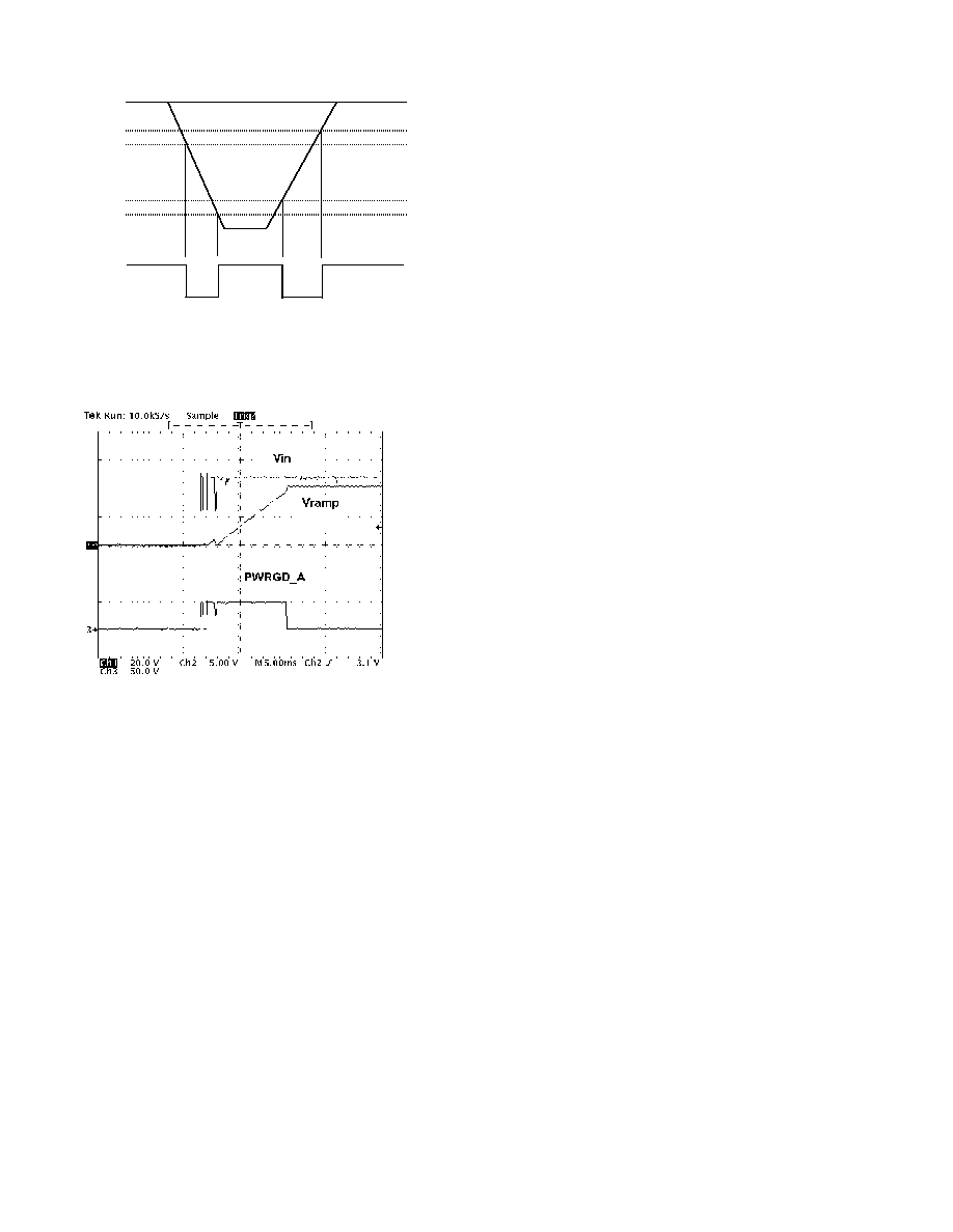
Undervoltage/Overvoltage Operation
GND
UV
OFF
UV
ON
Vin
OV
ON
OV
OFF
PWRGD SET RESET
Start-up Timing (PS11 PWRGD-A Active Low)
t
PWRGD-A
is the time delay from V
EEUV(on)
to PWRGD-A going
active. It can be approximated by
t
PWRGD-A
= C
RAMP
x (V
INT
-1.2)/I
RAMP
where
C
RAMP
= capacitor connected from RAMP pin to V
EE
pin
V
INT
= internal regulated power supply voltage (10V typ)
I
RAMP
= 10
µ
A charge current
PWRGD Flags Delay Programming
When the ramp voltage hits Vint ≠ 1.2V, PWRGD-A be-
comes active indicating that the input supply voltage is
within the programmed limits. PWRGD-B goes active after
a programmed time delay after PWRGD-A went active.
PWRGD-C goes active after a programmed time delay
after PWRGD-B went active. PWRGD-D goes active after
a programmed time delay after PWRGD-C went active.
The resistors connected from TB, TC, and TD to V
EE
pin
determines the delay times between the PWRGD flags.
The value of the resistors determines the capacitor charg-
ing and discharging current of a triangular wave oscillator.
The oscillator output is fed into an 8-bit counter to gener-
ate the desired time delay.
The respective time delay is defined by the following equa-
tion:
t
TX
= (255 x 2 x C
OSC
x V
PP
)/I
CD
and
I
CD
= Vbg / (4 x R
TX
)
Where
t
TX
= Time delay between respective PWRGD flags
C
OSC
= 120pF (internal oscillator capacitor)
V
PP
= 8.2V (peak-to-peak voltage swing of oscillator)
I
CD
= Charge and discharge current of oscillator
Vbg = 1.2V (internal band gap reference)
R
TX
= Programming resistor at TB, TC, or TD
Combining the two equations and solving for R
TX
yields:
R
TX
= (Vbg x t
TX
) / (2040 x C
OSC
x V
PP
)
= 0.6 x 10
6
x t
TX
For a time delay of 200ms
R
TX
= 0.6 x 10
6
x 0.2 = 120k
For a time delay of 5ms
R
TX
= 0.6 x 10
6
x 0.005 = 3k
PS10/PS11
7
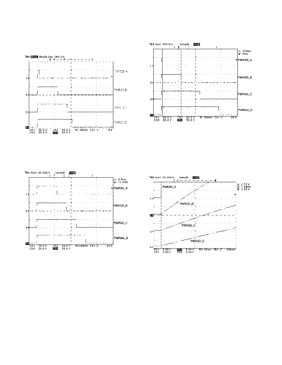
The following waveforms demonstrate the sequencing of
the PWRGD flags:
PWRGD Timing (PS11)
Test conditions: V
IN
= 48V, C
RAMP
= 10nF,
R
TB
= 121k, R
TC
= 60.4k, and R
TD
= 47.0k.
PWRGD Timing (Minimum Delays)
Test conditions: V
IN
= 48V, C
RAMP
= 10nF, R
TB
= 3.3k,
R
TC
= 3.3k, R
TD
= 3.3k, R
PULL-UP
= 47k.
PWRGD Timing (Maximum Delays)
Test conditions: V
IN
= 48V, C
RAMP
= 10nF, R
TB
= 121k,
R
TC
= 121k, R
TD
= 121k, R
PULL-UP
= 47k.
PS11 Power Down Sequence after UV
OFF
Test conditions: C
RAMP
= 10nF, R
TB
= 3.3k, R
TC
= 3.3k, R
TD
=
3.3k, R
PULL-UP
= 47k, C
PWRGD_B
= 0.47
µ
F, C
PWRGD_C
= 0.94
µ
F,
C
PWRGD_D
= 1.41
µ
F, V
UVOFF
= 33.4V, the assumed brick turn-
off threshold is 2.7V min TTL logic high. See power down
sequencing on Page 11.
Relative to Negative Rail
Relative to Negative Rail
Relative to Negative Rail
Relative to Negative Rail
PS10/PS11
8
PS11 Power Down Sequence after OV
OFF
Test conditions: C
RAMP
= 10nF, R
TB
= 3.3k, R
TC
= 3.3k, R
TD
=
3.3k, R
PULL-UP
= 47k, C
PWRGD_B
= 0.47
µ
F, C
PWRGD_C
= 0.94
µ
F,
C
PWRGD_D
= 1.41
µ
F, V
OVOFF
= 61.6V, the assumed brick turn-
off threshold is 2.7V min TTL logic high. See power down
sequencing on Page 11.
PWRGD Output Configuration
The PS10 and PS11 open drain power good outputs can be connected directly to the Enable pins of the DC/DC converter.
The internal pull-up and clamp of the DC/DC converter sets the logic High Enable/Disable voltage.
EN
UV
Notes:
1. Under Voltage Shutdown (UV) set to 35V.
2. Over Voltage Shutdown (OV) to 65V.
3. Other power good outputs will have the same
configuration as PWGRGD-A for Active High Enabled
Converters.
6.81K
PWRGD-B
V-
PS10
TADJ
TC
RTC
PWRGD-C
RTB
V+
V
TB
PWRGD-A
GND
RTD
10nF
-48V
+3.3V
PWRGD-D
COM
EE
487K
V
IN
9.76K
DC/DC
Converter
OV
TD
Ramp
Relative to Negative Rail
PS10/PS11
9
PWRGD Output Configuration, cont'd.
V+
-48V
6.81K
9.76K
Ramp
RTC
V-
IN
RTB
EE
PWRGD-A
RTD
PWRGD-D
TC
10nF
TD
Notes:
1. Under Voltage Shutdown (UV) set to 35V.
2. Over Voltage Shutdown (OV) to 65V.
3. Other power good outputs will have the same
configuration as PWGRGD-A for Active Low Enabled
Converters.
PS11
/EN
PWRGD-B
PWRGD-C
TADJ
TB
V
UV
V
OV
COM
487K
+3.3V
GND
DC/DC
Converter
Opto-isolated Enable
Some applications require opto-isolator interface to the Enable pin of the DC/DC converter. Make sure that the current transfer
ratio of the opto-coupler selected is at least 100% to ensure proper pull-down current on the Enable pin.
EE
GND
Notes:
1. Under Voltage Shutdown (UV) set to 35V.
2. Over Voltage Shutdown (OV) to 65V.
3. Other power good outputs will have the same
configuration as PWGRGD-A for Active High Enabled
Converters.
RTD
RTC
Ramp
6.81K
PWRGD-C
V
PWRGD-B
TD
EN
RTB
49.9k
TADJ
10nF
PWRGD-A
COM
V+
TB
V
+3.3V
PWRGD-D
487K
9.76K
V-
DC/DC
Converter
TC
UV
OV
IN
-48V
PS10
Opto-coupler
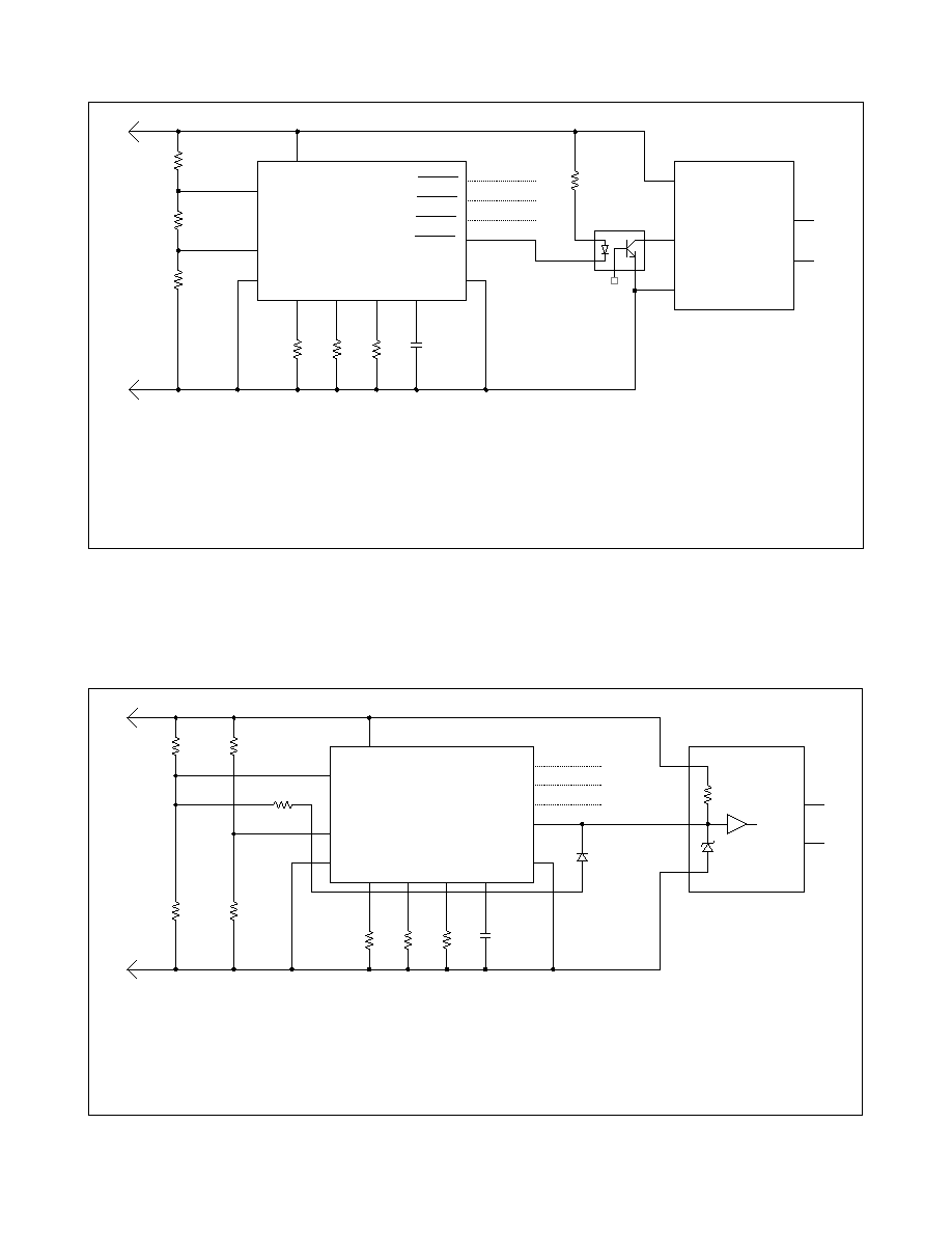
PS10/PS11
10
Opto-isolated Enable, cont'd.
49.9k
DC/DC
Converter
V-
UV
PWRGD-C
PWRGD-D
PS11
Notes:
1. Under Voltage Shutdown (UV) set to 35V.
2. Over Voltage Shutdown (OV) to 65V.
3. Other power good outputs will have the same
configuration as PWGRGD-A for Active Low Enabled
Converters.
+3.3V
TADJ
9.76K
RTD
-48V
10nF
Ramp
EE
V
OV
TC
IN
TD
RTB
6.81K
RTC
TB
Opto-coupler
COM
/EN
GND
487K
V+
PWRGD-B
V
PWRGD-A
Increasing the Under and Over Voltage Hysteresis
If the internal UV hysteresis is insufficient for a particular system application, then it may be increased by using separate resis-
tor dividers for UV and OV and providing a resistor feedback from UV pin to the PWRGD pin.
PS10
EN
TC
PWRGD-C
GND
9.76k
DC/DC
Converter
10nF
COM
V
16.5k
V
+3.3V
-48V
Ruvhys can be calculated based on higher UV On voltage (say
42V):
Ruvhys = (Vuvon - Vdiode - Vpwrgdlow)/((Vin-Vuvon)/487k -
Vuvon/16.5k)
= (1.26-0.65-0.4)/((42-1.26)/487k - 1.26/16.5k)
= 28.8k
TADJ
PWRGD-B
UV
V+
TB
TD
IN
487k
499k
PWRGD-A
V-
RTB
Note:
1. Other power good outputs will have the same configuration as
PWGRGD-A for Active High Enabled Converters.
Ruvhys
RTD
EE
RTC
OV
Ramp
PWRGD-D

PS10/PS11
11
Increasing the Under and Over Voltage Hysteresis, cont'd.
V
V+
Note:
1. Other power good outputs will have the same configuration as
PWGRGD-A for Active Low Enabled Converters.
TC
PWRGD-C
TADJ
Ramp
10nF
16.5k
V-
PWRGD-B
IN
V
10k
/EN
PWRGD-A
TD
9.76k
UV
RTB
RTD
EE
PS11
Ruvhys can be calculated based on higher UV On voltage (say
42V):
Ruvhys = (Vuvon - Vdiode - Vce/((Vin-Vuvon)/487k -
Vuvon/16.5k)
= (1.26-0.65-0.1)/((42-1.26)/487k - 1.26/16.5k)
= 69.9k
499k
COM
DC/DC
Converter
PWRGD-D
GND
Ruvhys
OV
RTC
+3.3V
-48V
TB
487k
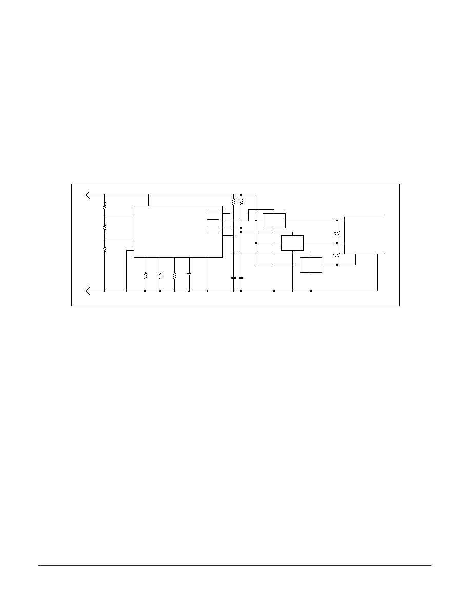
Power Down Sequencing
In some applications, a power down sequence may be required. To accomplish this, a capacitor is connected to the power
good pins that need to be sequenced down. The power good turn off delays can be approximated by
T
PWRGD-B(off)
= C1 x V
ENOFF
/ I
PULLUP
,
T
PWRGD-C(off)
= C2 x V
ENOFF
/ I
PULLUP
,
T
PWRGD-D(off)
= C3 x V
ENOFF
/ I
PULLUP
,
where:
T
PWRGD-B(off)
-Time delay from PWRGD-A going High to PWRGD-B going high.
T
PWRGD-c(off)
-Time delay from PWRGD-A going High to PWRGD-C going high.
T
PWRGD-D(off)
-Time delay from PWRGD-A going High to PWRGD-D going high.
V
ENOFF
- DC/DC minimum off voltage (2.7V typ)
I
PULLUP
- DC/DC /EN pin pull-up current (1mA typ)
Note: Adding C1, C2, C3 will have a negligible affect on the power good fall time.
487K
RTC
TB
V
/EN
C1
RTD
OV
TC
Notes:
1. Under Voltage Shutdown (UV) set to 35V.
2. Over Voltage Shutdown (OV) to 65V.
3. Only PWRGD-A to DC/DC converter connection is shown
for simplicity.
9.76K
PWRGD-A
Ramp
V
TADJ
RTB
PS11
C3
6.81K
/EN2
C2
PWRGD-C
TD
COM
IN
V+
PWRGD-B
/EN3
GND
+3.3V
DC/DC
Converter
-48V
10nF
UV
EE
PWRGD-D
/EN4
V-
PS10/PS11
12
PS10 Power Good Clamp
If the active high enabled dc/dc converter used does not have an internal clamp, an external zener diode may be used to pro-
tect the module.
RTB
6.81K
9.76K
49.9k
V
PWRGD-B
Notes:
1. Under Voltage Shutdown (UV) set to 35V.
2. Over Voltage Shutdown (OV) to 65V.
3. Other power good outputs will have the same
configuration as PWGRGD-A for Active High Enabled
Converters.
V-
GND
EN
RTD
COM
TD
UV
TADJ
10nF
+3.3V
IN
TB
-48V
Ramp
TC
PWRGD-D
PS10
OV
RTC
PWRGD-C
V
EE
DC/DC
Converter
V+
487K
PWRGD-A
Extending the PWRGD-A time Delay
The time delay from UV high to PWRGD-A active can be extended by connecting a low impedance voltage source like a DAC
output during start-up. A voltage 0 to 50mV applied to the TADJ pin will reduce the 10
µ
A Cramp charging current according to:
I
RAMP
= 10
µ
A ≠ V
TADJ
/5K
Reducing the charging current will extend the PWRGD-A delay by:
T
PWRGD-A
= (C
RAMP
x 8.8V)/(10
µ
A ≠ V
TADJ
/5K)
Rearranging the equation
V
TADJ
= 5k x (10
µ
A ≠ C
RAMP
x 8.8V/ T
PWRGD-A
)
For a 20ms delay, for example,
V
TADJ
= 5k x (10
µ
A ≠ 10nF x 8.8V/ 20ms
) = 0.028V
/EN
UV
PWRGD-B / PWRGD-B
-
1
5
7
+12V
0 - 50mV
DAC
/EN
PWRGD-D / PWRGD-D
+
IN
2
-48V or GND
EE
PS10/PS11
10V
3
RTD
COM
+
V
GND or +48V
6.81K
Notes:
1. Under Voltage Shutdown (UV) set to 35V.
2. Over Voltage Shutdown (OV) to 65V.
14
TC
13
COM
DC/DC
Converter
TD
11
DC/DC
Converter
10nF
/EN
COM
-
TB
6
10uA
+2.5V
DC/DC
Converter
+3.3V
10
COM
RTC
4
9.76K
+5V
V
PWRGD-A / PWRGD-A
487K
5k
DC/DC
Converter
PWRGD-C / PWRGD-C
/EN
8
RTB
OV
TADJ
Ramp
12
PS10/PS11
13
Typical Application Circuit for a 12V Non-Isolated System
Most FPGAs, Processors, ASICs, and DSPs require sequencing and rail voltage limititation during start-up and power down
sequence of its rails. A typical requirement is: V
DD
_CORE must not exceed V
DD
_IO more than 0.6V and V
DD
_IO must not ex-
ceed V
IN
at any time. This can be accomplished by sequencing the dc/dc converters by the following manner:
Turn On: V
DD
_CORE first, V
DD
_IO second, and V
IN
last.
Tun-Off: V
IN
first, V
DD
_IO second, and V
DD
_CORE last.
The Schottky diodes will limit the voltage between the rails to around 0.3V @ 3A during the power-up and power-down se-
quence.
Assuming that the /EN pins of the dc/dc converters have no pull-up and have a 1.0V turn-off threshold, the power-down se-
quence time delays can be approximated by:
T
PWRGD-C
to T
PWRGD-B
= 1
µ
F x 1V / 1mA = 1ms
T
PWRGD-B
to T
PWRGD-A
= (2
µ
F-1
µ
F) x 1V / 1mA = 1ms
C2
1uF
IN
10nF
VIN
30BQ015
R9
12k
6
V
RTD
PWRGD-C
12
EE
PS11
Buck
Converter
TD
VDD_IO
R3
30BQ015
2
14
PWRGD-A
5
Ramp
13
7
R2
/EN
1
3
TB
GND
/EN
TC
10
GND
RTC
Buck
Converter
TADJ
RTB
OV
+12V
R1
VDD_CORE
+2.5V
V
C1
2uF
R8
12k
+5V
8
LOAD
PWRGD-B
/EN
PWRGD-D
+3.3V
UV
Buck
Converter
11
4
Supertex inc.
©2003 Supertex Inc. All rights reserved. Unauthorized use or reproduction prohibited.
1225 Bordeaux Drive, Sunnyvale, CA 94089
TEL: (408) 222-8888 ∑ FAX: (408) 222-4895
www.supertex.com
04/07/03rev7b