1
03/12/02
Supertex Inc. does not recommend the use of its products in life support applications and will not knowingly sell its products for use in such applications unless it receives an adequate "products liability
indemnification insurance agreement." Supertex does not assume responsibility for use of devices described and limits its liability to the replacement of devices determined to be defective due to
workmanship. No responsibility is assumed for possible omissions or inaccuracies. Circuitry and specifications are subject to change without notice. For the latest product specifications, refer to the
Supertex website: http://www.supertex.com. For complete liability information on all Supertex products, refer to the most current databook or to the Legal/Disclaimer page on the Supertex website.
Absolute Maximum Ratings
Supply voltage, V
DD
1
-0.5V to +7.5V
Output Voltage, V
NN
1
V
DD
+ 0.5V to -95V
Logic input levels
1
-0.3V to V
DD
+0.3V
Ground Current
2
1.5A
Continuous total power dissipation
3
Plastic
1200mW
Ceramic
1900mW
Operating temperature range
Plastic
-40
∞
C to +85
∞
C
Ceramic -55
∞
C to +125
∞
C
Storage temperature range
-65
∞
C to +150
∞
C
Lead temperature 1.6mm (1/16 inch)
from case for 10 seconds
260
∞
C
Notes:
1. All voltages are referenced to V
SS
.
2. Limited by the total power dissipated in the package.
3. For operation above 25
∞
C ambient derate linearly to maximum operating
temperature at 20mW/
∞
C for plastic and at 19mW/
∞
C for ceramic.
HV57009
64-Channel Serial To Parallel Converter
With P-Channel Open Drain Controllable Output Current
General Description
The HV570 is a low-voltage serial to high-voltage parallel con-
verter with P-channel open drain outputs. This device has been
designed for use as a driver for plasma panels.
The device has two parallel 32-bit shift registers, permitting data
rate twice the speed of one (they are clocked together). There
are also 64 latches and control logic to perform the blanking of
the outputs. HV
OUT
1 is connected to the first stage of the first shift
register through the blanking logic. Data is shifted through the
shift registers on the logic low to high transition of the clock. The
DIR pin causes CCW shifting when connected to V
SS
, and CW
shifting when connected to V
DD
. A data output buffer is provided
for cascading devices. This output reflects the current status of
the last bit of the shift register (HV
OUT
64). Operation of the shift
register is not affected by the LE (latch enable), or the BL
(blanking) inputs. Transfer of data from the shift registers to
latches occurs when the LE input is high. The data in the latches
is stored when LE is low.
The HV570 has 64 channels of output constant current sourcing
capability. They are adjustable from 0.1 to 2.0mA through one
external resistor or a current source.
Features
Processed with HVCMOS
Æ
technology
5V CMOS Logic
Output voltage up to -85V
Output current source control
16MHz equivalent data rate
Latched data outputs
Forward and reverse shifting options (DIR pin)
Diode to V
DD
allows efficient power recovery
Hi-Rel processing available
Package Options
Device
80-Lead Quad
Ceramic Gullwing
80 Lead Quad
Plastic Gullwing
Die
80 Lead Quad
Ceramic Gullwing
(MIL-Std-833 Processed*)
HV57009
HV57009DG
HV57009PG
HV57009X
RBHV57009DG
* For Hi-Rel process flows, refer to page 5-3 of the Databook.
Ordering Information

2
Symbol
Parameter
Min
Max
Units
Conditions
I
DD
V
DD
supply current
15
mA
V
DD
= V
DD
, max
f
CLK
= 8MHz
I
NN
High voltage supply current
-10
µ
A
Outputs off, HV
OUT
= -85V
(total of all outputs)
I
DDQ
Quiescent V
DD
supply current
100
µ
A
All inputs = V
DD
, except
+IN = V
SS
= GND
V
OH
High-level output
Data out
V
DD
-0.5
V
I
O
= -100
µ
A
HV
OUT
+1
V
DD
V
I
O
= -2mA
V
OL
Low-level output
Data out
+0.5
V
I
O
= 100
µ
A
I
IH
High-level logic input current
1
µ
A
V
IH
= V
DD
I
IL
Low-level logic input current
-1
µ
A
V
IL
= 0V
I
CS
HV output source current
-2
mA
V
REF
= 2V, R
EXT
= 1K,
see Figures 8a and 8b
-0.1
mA
V
REF
= 0.1V, R
EXT
= 1K,
see Figure 8a and 8b
I
CS
HV output source current for I
REF
= 2.0mA
10
%
V
REF
= 2V, R
EXT
= 1K
Electrical Characteristics
DC Characteristics
(All voltages are referenced to V
SS
, V
SS
= 0, TA = 25
∞
C)
Symbol
Parameter
Min
Max
Units
Conditions
f
CLK
Clock frequency
DC
8
MHz
Per register
t
WL
, t
WH
Clock width high or low
62
ns
t
SU
Data set-up time before clock rises
10
ns
t
H
Data hold time after clock rises
15
ns
t
ON
, t
OFF
Time for latch enable to HV
OUT
500
ns
C
L
= 15pF
t
DHL
Delay time clock to data high to low
70
ns
C
L
= 15pF
t
DLH
Delay time clock to data low to high
70
ns
C
L
= 15pF
t
DLE
Delay time clock to LE low to high
25
ns
t
WLE
Width of LE pulse
25
ns
t
SLE
LE set-up time before clock rises
0
ns
t
r
, t
f
Maximum allowable clock rise and fall time
100
ns
(10% and 90% points)
AC Characteristics
(Logic signal inputs and Data inputs have t
r
, t
f
5ns [10% and 90% points] for measurements)
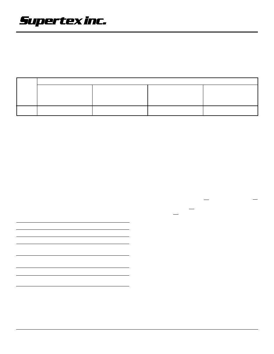
Notes 1: Current going out of the chip is considered negative.
HV57009
3
HV57009
V
DD
Input
Logic Inputs
Data Out
Logic Data Output
V
DD
V
DD
Input
To Internal
Circuits
V
SS
V
SS
V
SS
Analog Input
V
DD
I
CS
HV
OUT
P
CTL
High Voltage Output
Symbol
Parameter
Min
Max
Units
V
DD
Logic supply voltage
4.5
5.5
V
HV
OUT
HV output off voltage
-85
V
DD
V
V
IH
High-level input voltage
V
DD
- 1.2V
V
DD
V
V
IL
Low-level input voltage
0
1.2
V
f
CLK
Clock frequency per register
DC
8
MHz
T
A
Operating free-air temperature
Plastic
-40
+85
∞
C
Ceramic
-55
+125
∞
C
Note:
Power-up sequence should be the following:
1. Connect ground.
2. Apply V
DD
.
3. Set all inputs to a known state.
Power-down sequence should be the reverse of the above.
Recommended Operating Conditions
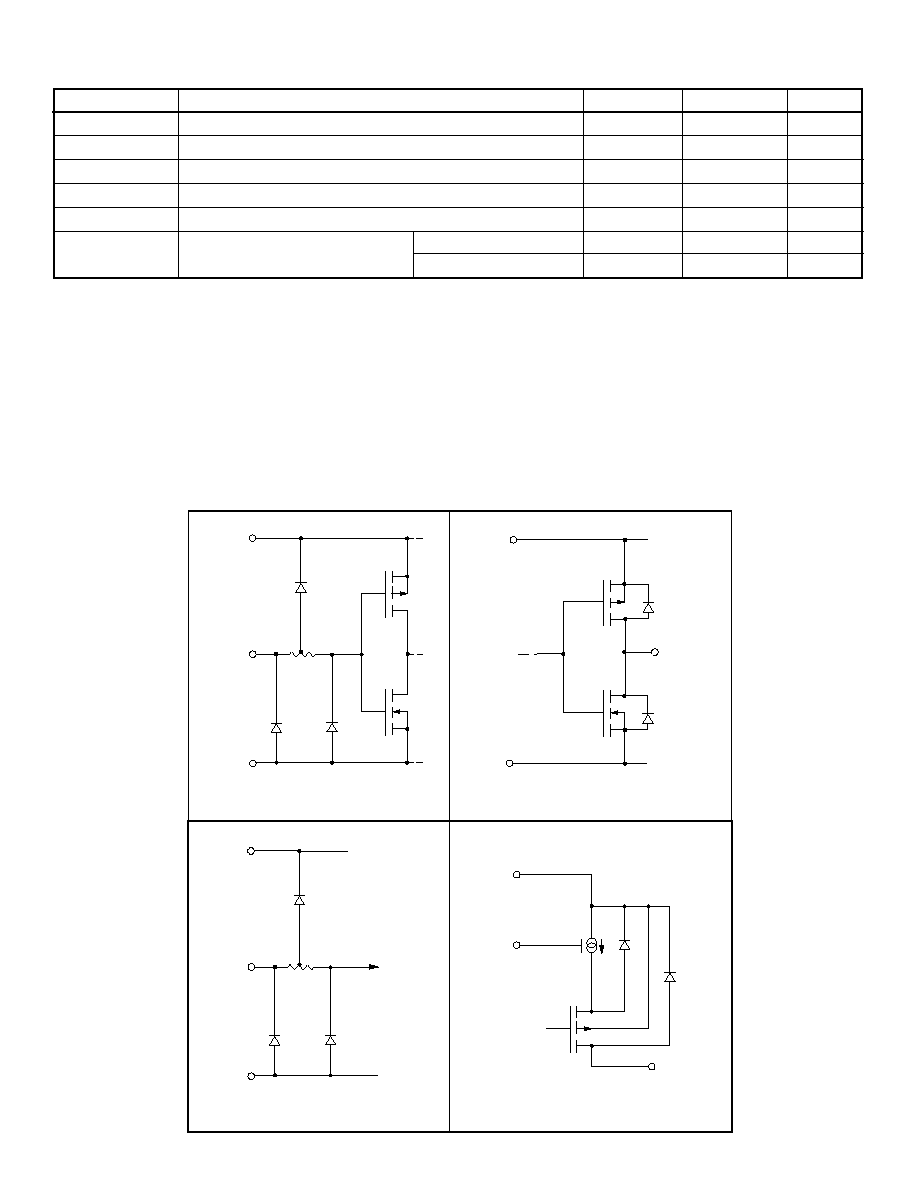
Figure 1: Input and Output Equivalent Circuits
4
HV57009
LE
HV
OUT
w/ data input
LOW
Previous I
O
= I
REF
Previous I
O
= 0
I
O
= 0
I
O
= I
REF
Data Valid
50%
50%
Data Input
CLK
Data Out
50%
50%
50%
t
SU
t
H
t
WL
t
WH
50%
t
DLH
t
DHL
50%
t
WLE
t
DLE
t
SLE
50%
50%
t
ON
10%
HV
OUT
w/ data input
HIGH
90%
90%
10%
t
OFF
V
DD
V
SS
V
DD
V
SS
V
DD
V
SS
V
DD
V
SS
V
DD
V
SS
V
DD
HV
OUT
(off)
V
DD
HV
OUT
(off)
10%
90%
90%
10%
50%
t
f
t
r
Figure 2: Switching Waveforms
5
HV57009
HV
OUT
1
HV
OUT
2
HV
OUT
3
∑
∑
∑
HV
OUT
33
HV
OUT
34
HV
OUT
35
∑
∑
∑
Latch
Latch
Latch
Latch
Programmable
Current
V
DD
V
SS
BL
LE
SR2
SR1
CLK
DIR
V
BP
+IN
-IN
HV
OUT
32
HV
OUT
64
D
I/O
2A D
I/O
1A
D
I/O
2B D
I/O
1B
I/O
I/O
Inputs
Outputs
Function
Data In
CLK
LE
BL
DIR
Shift Reg
HV Outputs
Data Out
All O/P High
X
X
L
H
H
H
H
Data Stored in Latches
X
L
H
I/O Relation
H
H
L
H
L
H
H
H
X
L
H
X
D
I/O
1-2A
D
I/O
1-2A
D
I/O
1-2B
D
I/O
1-2B
Figure 4: Function Table
X
X
X
X
H
H
L
L
*
L....L
H....H
*
Q
n
Q
n+1
Q
n
Q
n+1
Q
n
Q
n-1
Q
n
Q
n-1
ON
ON
OFF
New ON or OFF
Previous ON or OFF
Previous ON or OFF
New ON or OFF
Notes:
* = dependent on previous stage's state. See Figure 7 for D
IN
and D
OUT
pin designation for CW and CCW shift.
H = V
DD
(Logic)/V
NN
(HV Outputs)
L = V
SS
Note: Each SR (shift register) provides 32 outputs. SR1 supplies outputs 1 to 32 and SR2 supplies outputs 33 to 64.
Figure 3: Functional Block Diagram
Inversion of
Stored Data
Data Falls Through
(Latches Tansparent)
*
L
H
*
D
I/O
1-2B
D
I/O
1-2B
D
I/O
1-2A
D
I/O
1-2A
6
HV57009
65
80
1
24
25
40
41
64
Index
top view
80-pin Gullwing Package
25
26
36
37
HV 32
∑
∑
∑
∑
∑
HV 2
HV 1
HV 33
∑
∑
∑
∑
∑
HV 63
HV 64
Pin
SR1
SR2
OUT
OUT
OUT
OUT
OUT
OUT
DIR = VDD; CW (HVOUT1
HVOUT64)
DIR = VSS; CCW (HVOUT64
HVOUT1)
CW
CW
Pin
Function
1
HV
OUT
24
2
HV
OUT
23
3
HV
OUT
22
4
HV
OUT
21
5
HV
OUT
20
6
HV
OUT
19
7
HV
OUT
18
8
HV
OUT
17
9
HV
OUT
16
10
HV
OUT
15
11
HV
OUT
14
12
HV
OUT
13
13
HV
OUT
12
14
HV
OUT
11
15
HV
OUT
10
16
HV
OUT
9
17
HV
OUT
8
18
HV
OUT
7
19
HV
OUT
6
20
HV
OUT
5
21
HV
OUT
4
22
HV
OUT
3
23
HV
OUT
2
24
HV
OUT
1
25
D
I/O
1A
26
D
I/O
2A
27
N/C
28
N/C
29
LE
30
CLK
31
BL
32
V
SS
33
DIR
34
V
DD
35
-IN
36
D
I/O
2B
37
D
I/O
1B
38
N/C
39
+IN
40
V
BP
Figure 5: Pin Configurations
80-pin Gullwing Package
Pin
Function
41
HV
OUT
64
42
HV
OUT
63
43
HV
OUT
62
44
HV
OUT
61
45
HV
OUT
60
46
HV
OUT
59
47
HV
OUT
58
48
HV
OUT
57
49
HV
OUT
56
50
HV
OUT
55
51
HV
OUT
54
52
HV
OUT
53
53
HV
OUT
52
54
HV
OUT
51
55
HV
OUT
50
56
HV
OUT
49
57
HV
OUT
48
58
HV
OUT
47
59
HV
OUT
46
60
HV
OUT
45
61
HV
OUT
44
62
HV
OUT
43
63
HV
OUT
42
64
HV
OUT
41
65
HV
OUT
40
66
HV
OUT
39
67
HV
OUT
38
68
HV
OUT
37
69
HV
OUT
36
70
HV
OUT
35
71
HV
OUT
34
72
HV
OUT
33
73
HV
OUT
32
74
HV
OUT
31
75
HV
OUT
30
76
HV
OUT
29
77
HV
OUT
28
78
HV
OUT
27
79
HV
OUT
26
80
HV
OUT
25
Figure 6: Package Outline
Figure 7: Shift Register Operation
Notes:
1. Pin designation for DIR = V
DD
.
2. A 0.1
µ
F capacitor is needed between V
DD
and V
BP
(pin 40) for better output
current stability and to prevent transient cross-coupling between outputs.
See Fig. 8a and 8b.
DIR = V
DD
:
D
I/O
1A
D
I/O
2A
D
I/O
2B
D
I/O
1B
DIR = V
SS
:
D
I/O
2A
D
I/O
1A
D
I/O
1B
D
I/O
2B

7
HV57009
I
OUT
HV
OUT
V
DD
V
REF
I
REF
R
EXT
+IN
-IN
R
D
*
10K
C
D
*
390pF
HV570
Logic
To other
outputs
- +
0.1
µ
F
V
BP
V
SS
V
REF
I
OUT
HV
OUT
V
DD
0.1
µ
F
V
BP
I
REF
R
EXT
+IN
-IN
R
D
*
10K
C
D
*
390pF
HV570
Logic
To other
outputs
- +
V
SS
Since I
OUT
= I
REF
=
Therefore, if I
OUT
= 2mA and V
REF
= -5V
R
EXT
= 2.5K
.
If I
OUT
= 1mA and R
EXT
= 1K
V
REF
= -1V.
If R
EXT
>10K
, add series network R
D
and C
D
to ground for
stability as shown.
This control method behaves linearly as long as the operational
amplifier is not saturated. However, it requires a negative power
source and needs to provide a current I
REF
= I
OUT
for each HV570
chip being controlled.
If HV
OUT
+1V, the HV
OUT
cascode may no longer operate as a
perfect current source, and the output current will diminish. This
effect depends on the magnitude of the output current.
Given I
OUT
and V
REF
, the R
EXT
can be calculated by using:
R
EXT
=
V
REF
=
V
REF
I
REF
I
OUT
The intersection of a set of I
OUT
and V
REF
values can be located
in the graph shown below. The value picked for R
EXT
must always
be in the shaded area for linear operation. This control method
has the advantage that V
REF
is positive, and draws only leakage
current. If R
EXT
> 10K, add series network R
D
and C
D
to ground
for stability as shown.
Note: Lower reference current I
REF
, results in higher distortion,
I
CS
, on the output.
*Required if R
EXT
> 10K or R
EXT
is replaced by a constant
current source.
Typical Current
Programming Circuits
Figure 8b: Positive Control
Figure 8a: Negative Control
V
REF
R
EXT
1
2
3
4
5
3
4
5
6
7
8
2
1
0
I OUT
(mA)
VREF (V)
100
250
500
REXT = 1K
5K
2K
1235 Bordeaux Drive, Sunnyvale, CA 94089
TEL: (408) 744-0100 ∑ FAX: (408) 222-4895
www.supertex.com
03/12/02
©2001 Supertex Inc. All rights reserved. Unauthorized use or reproduction prohibited.