 | –≠–ª–µ–∫—Ç—Ä–æ–Ω–Ω—ã–π –∫–æ–º–ø–æ–Ω–µ–Ω—Ç: SR087 | –°–∫–∞—á–∞—Ç—å:  PDF PDF  ZIP ZIP |
Supertex inc.
Supertex inc.
∑
1235 Bordeaux Drive, Sunnyvale, CA 94089
∑
Tel: (408) 222-8888
∑
FAX: (408) 222-4895
∑
www.supertex.com
1
NR040306
SR086/SR087
Initial Release
Adjustable Off-Line
Inductorless Switching Regulator
Features
Effi cient operation without magnetics
No high voltage capacitors
Adjustable main output voltage (9V to 50V)
Additional 3.3V or 5V internal regulator
Up to 100mA combined output current
Single BOM for 120VAC/230VAC
Built-in soft start
Less than 200mW standby power
Applications
White goods
Household appliances
Lighting controls
Circuit breakers
Keep-alive supplies
General Description
The Supertex SR08x is an inductorless switching regulator
designed to operate directly from a rectifi ed AC line. The
operating principle is to turn on a pass transistor when the
rectifi ed AC is below the output voltage, and to turn it off when
the output voltage reaches a specifi c level. A linear regulator
supplied by V
OUT
provides an additional fi xed 3.3V output
(SR086) or 5V output (SR087). Effi ciencies of around 55%
may be realized for loads up to 1W in 120VAC applications,
with around 50% effi ciencies for loads up to 800mW in 230VAC
applications.
A logic-level enable input allows the SR08x to be disabled
≠ useful when the SR08x is employed as a keep-alive power
supply.
WARNING! Galvanic isolation is not provided. Dangerous
voltages are present when connected to the AC line. It is
the responsibility of the designer employing the SR08x
to ensure adequate safeguards are in place to protect the
end user from electrical shock.
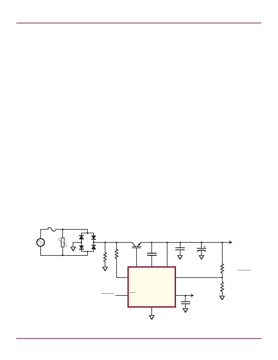
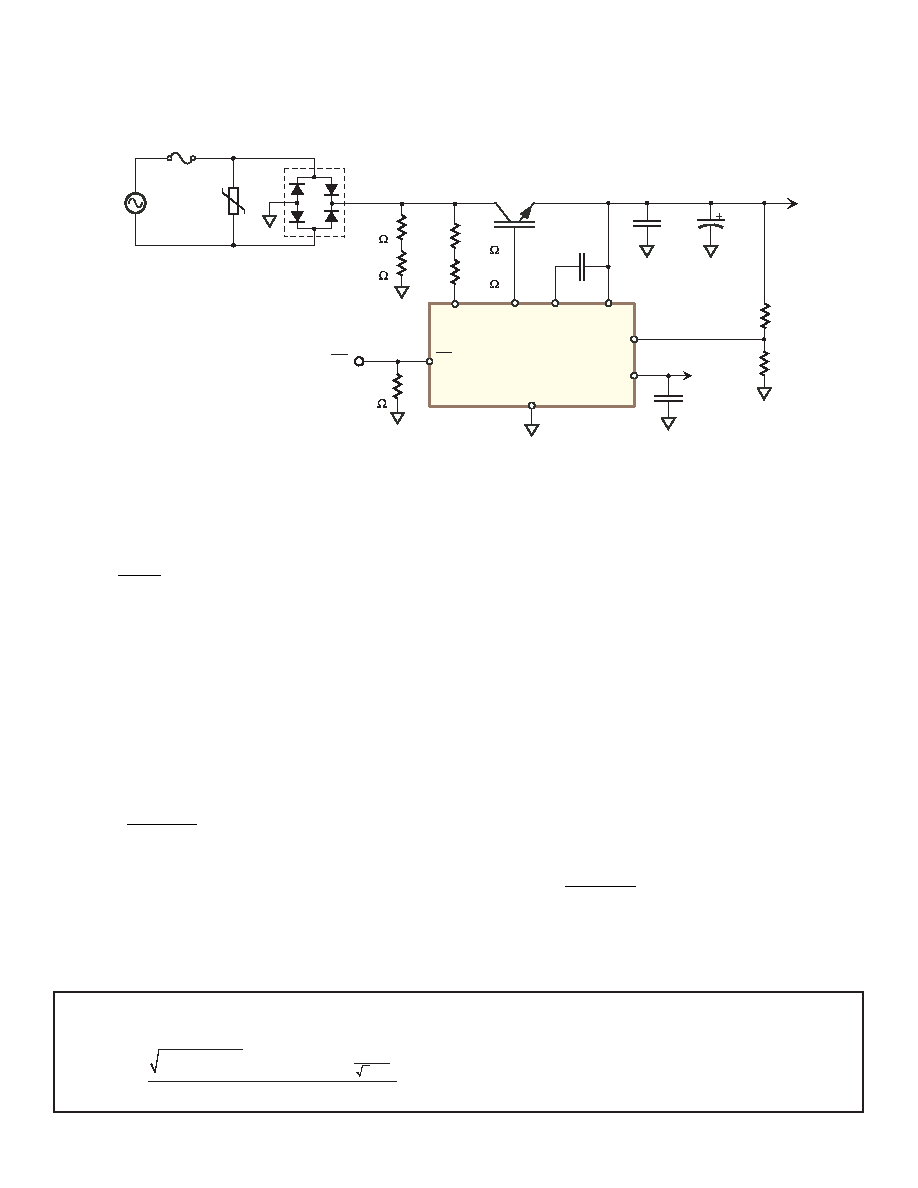
Typical Application Circuit
FB
V
REG
V
OUT
9-50VDC
@ 100mA - I
REG
SR08x
R
2
12.4k
EN
GND
V
IN
GATE
V
OUT
3.3V or 5V
@ 60mA
V
GD
470F
1F
100nF
100nF
Enable
1.25A
STGD5NB120SZ
R
1
275V
50A
1.0kV
1A
390k
1.1M
= R
2
V
OUT
1.25V
1
-
90VAC
to
270VAC
50/60HZ
2
NR040306
SR086/SR087
Device (V
REG
)
Package Options
8-Lead SOIC
SR086 (3.3V)
SR086SG-G
SR087 (5.0V)
SR087SG-G
-G indicates package is RoHS compliant (`Green')
Absolute Maximum Ratings
Parameter
Value
Output Voltage (V
OUT
)
-0.3V to 56V
Feedback Voltage (V
FB
)
-0.3V to 6.5V
Enable Voltage (V
EN
)
-0.3V to 6.5V
Operating Junction Temperature
-40
o
C to +125
o
C
Symbol
Parameter
Min
Typ
Max
Units
Conditions
Recommended Operating Conditions
Absolute Maximum Ratings are those values beyond which damage to the
device may occur. Functional operation under these conditions is not implied.
Continuous operation of the device at the absolute rating level may affect device
reliability. All voltages are referenced to device ground.
Pinout
SO-8
GATE
V
GD
V
OUT
V
FB
V
REG
GND
EN
V
IN
Heat Slug
Backside on the SO-8 package is at ground potential and may be connected
to ground or left unconnected.
Name
Pin #
Description
V
IN
1
Rectifi ed AC input voltage
EN
2
Active low enable input
GND
3
Circuit ground
Note: circuit ground will be at the AC line potential
V
REG
4
Regulated output voltage, fi xed 3.3V or
5.0V
FB
5
Feedback input
V
OUT
6
Output voltage (9.0V - 50V adj.)
V
GD
7
Gate drive supply (referenced to V
OUT
)
GATE
8
Drives external IGBT pass transistor
V
OUT
Output voltage
9
-
50
V
---
I
OUT
Load on V
OUT
including feedback divider and load
on V
REG
100
-
-
µA
---
Specifi cations
(Unless otherwise noted, T
A
= -40∞C to +85∞C, Voltages referenced to GND pin)
Symbol
Parameter
Min
Typ
Max
Units
Conditions
I
GD
Current consumption at V
GD
-
-
60
µA
---
I
OUT(int)
Current consumption of the lower
circuitry
-
-
400
µA
V
OUT
= 9-50V
V
GD
Gate drive supply voltage
1
11
13
15
V
---
V
GATE(hi)
GATE output high voltage
1
11
-
15
V
---
V
GATE(lo)
GATE output low voltage
1
-
-
0.5
V
---
V
FB(off)
Feedback voltage (GATE off)
1.18
1.25
1.31
V
---
V
FB(hys)
Feedback voltage hysteresis
-
50
-
mV
---
Ordering Options
Pin Description
3
NR040306
SR086/SR087
I
FB
FB input current
-
-
500
nA
---
V
TRIP(on)
V
IN
trip voltage, GATE on
1
0
-
3
V
---
V
TRIP(off)
V
IN
trip voltage, GATE off
1
9
-
15
V
---
V
EN(on)
Enable voltage, on
0.2
-
-
V
---
V
EN(off)
Enable voltage, off
-
-
0.75
V
REG
---
t
DIG(on)
V
IN
≠ GATE turn-on delay
0
-
1.0
µs
C
GATE
= 1nF
t
DIG(off)
V
IN
≠ GATE turn-off delay
-
-
600
ns
C
GATE
= 1nF
t
DFG(off)
FB ≠ GATE turn-off delay
-
-
450
ns
C
GATE
= 1nF V
FB
= 1.5V
V
REG
Regulated output voltage SR086
SR087
3.125
4.750
3.300
5.000
3.465
5.250
V
I
LOAD
= 1mA, V
OUT
= 9V
I
V
REG
V
REG
load regulation
-50
-
+50
mV
0mA < I
LOAD
< 60mA, V
OUT
= 9V,
T
Amb
= 25∞C
V
D
GATE ≠ V
GD
diode drop
-
-
800
mV
I = 20mA
Specifi cations (cont.)
Symbol
Parameter
Min
Typ
Max
Units
Conditions
1
Referenced to V
OUT.
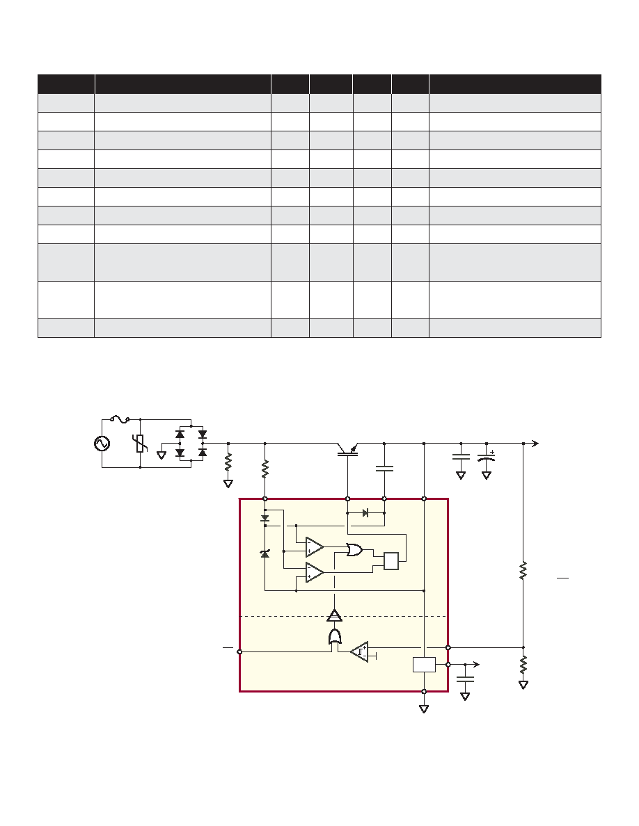
Block Diagram
V
GD
V
IN
GATE
V
OUT
1.25V
GND
FB
Reg
3.3V/5V
V
REG
9VDC to
50VDC
13V
Upper circuitry
powered by V
GD
V
OUT
level
translator
R
S
Q
90VAC to
270VAC
50/60Hz
Lower circuitry
powered by V
OUT
GND
EN
SR08x
R
FBlo
12.4k
C
OUT
470
F
C
OUT1
1.0
F
C
GD
100nF
1.25A
STGD5NB120SZ
1.0kV
1A
R
PD
390k
R
GD
1.1M
275V
50A
R
FBhi
C
REG
100nF
= R
FBlo
(
V
OUT
- 1
)
1.25V
4
NR040306
SR086/SR087
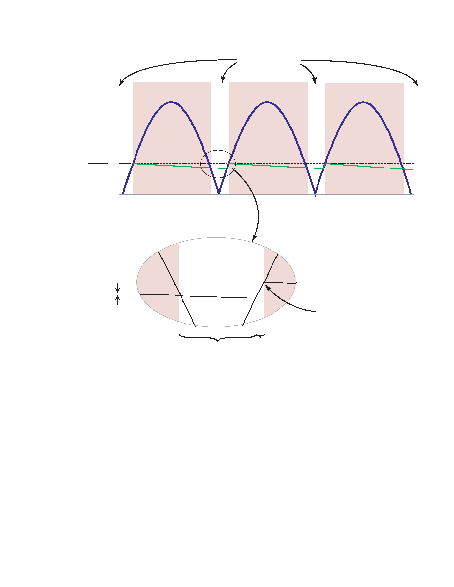
SR08x Timing
V
OUT
V
IN
Pass Transistor on
not to scale
Pass Transistor is turned
on when V
IN
falls below:
V
OUT
+V
TRIP(ON)
V
FB(OFF)
(
1+
)
RF
Bhi
RF
Blo
Pass Transistor is on but
not conducting since the
input voltage is lower
than the output voltage
Pass Transistor is
on and conducting
Pass Transistor is
turned off once V
OUT
reaches the trip point
5
NR040306
SR086/SR087
Data Sheet Application Section:
Typical Application Circuit
Output Voltage*
V
OUT
may be adjusted in the range of 9V to 50V*, by changing
feedback resistor R
5
according to the following equation.
Leave R
6
at 12.4k or less - it assures a minimum 100µA
load required for the proper operation of the SR087. Change
R
3
and R
4
according to the R
3
+R
4
equation below. Select
C
2
and C
3
with appropriate voltage ratings. For C
3
, use a
low ESR capacitor with an adequate ripple current rating
(800mA
RMS
). Use ceramic for C
2
.
Since V
REG
is a linear regulator supplied from V
OUT
, the maxi-
mum current available from V
REG
is reduced as V
OUT
is in-
creased due to power considerations.
or 60mA, whichever is less.
Input Voltage
To reduce standby power for 230VAC-only applications,
or for supply voltages less than 90Vrms, R
3
and R
4
should
be changed according to the R
3
+R
4
equation below. R
1
+R
2
should remain at 400k or less.
Two resistors in series
are employed to ensure adequate creepage distances for
230VAC operation. For 120VAC-only applications, single re-
sistors may be employed.
Output Ripple*
Storage capacitor C
3
was sized to provide about 2V
P-P
ripple
at 100mA load (I
OUT
+ I
REG
). For lighter loads, C
3
may be re-
duced. Conversely, C
3
may be increased for lower ripple.
Use a low ESR capacitor with an adequate ripple current
rating (800mA
RMS
for 100mA loads). Effi ciency and output
current capability may drop with increased capacitance be-
cause of a smaller conduction angle associated with lower
ripple. Due to feedback hysteresis, ripple cannot be reduced
below 4%.
*V
REG
requires at least 4V of headroom. Therefore, V
OUT
, including ripple,
must not fall below 9V for the SR087, or below 7.3V for the SR086.
R
R
V
OUT
5
6
1 25
1
=
-
.
V
I
V
REG(max)
OUT
=
-
1 5
5
. W
V
V
I
I
f C
RIPPLE P P
OUT
REG
IN
(
)
-
+
2
3
R
3
+ R
4
Equation:
R
R
V
X
V
V
X
IN
3
4
1
2
25
+
(
)
<
( )
-
cos
A
2V
IN
2
- V
X
2
-
where V
X
= V
OUT
+ 15V
Use the minimum anticipated RMS value for V
IN
.
Take resistor tolerance into account, selecting the
next lower standard value. Choosing a lower value
has no effect other than higher standby power.
V
GD
V
IN
GATE
V
OUT
GND
FB
V
REG
5VDC
V
REG
V
OUT
12.6VDC
V
IN
90VAC to
270VAC
50/60Hz
EN
*R
3
510k
*R
1
200k
C
1
100nF
C
2
1.0µF
C
3
470µF
R
5
113k
R
6
12.4k
R
7
100k
D
1
1.0kV
1A
Z
1
275V
50A
F
1
1.00A
EN
Q
1
STGD5NB120SZ
*R
2
200k
*R
4
510k
1
2
4
3
5
6
7
8
C
4
100nF
IC
1
SR087
* Two resistors used in
series for reasons of
high voltage creepage
and resistor voltage
rating.