 | –≠–ª–µ–∫—Ç—Ä–æ–Ω–Ω—ã–π –∫–æ–º–ø–æ–Ω–µ–Ω—Ç: TN2106K1 | –°–∫–∞—á–∞—Ç—å:  PDF PDF  ZIP ZIP |
7-71
TN2106
Advanced DMOS Technology
These enhancement-mode (normally-off) transistors utilize a
vertical DMOS structure and Supertex's well-proven silicon-gate
manufacturing process. This combination produces devices with
the power handling capabilities of bipolar transistors and with the
high input impedance and positive temperature coefficient inher-
ent in MOS devices. Characteristic of all MOS structures, these
devices are free from thermal runaway and thermally-induced
secondary breakdown.
Supertex's vertical DMOS FETs are ideally suited to a wide range
of switching and amplifying applications where high breakdown
voltage, high input impedance, low input capacitance, and fast
switching speeds are desired.
Note: See Package Outline section for dimensions.
Package Options
BV
DSS
/
R
DS(ON)
V
GS(th)
BV
DGS
(max)
(max)
TO-236AB*
TO-92
Die
60V
2.5
2.0V
TN2106K1
TN2106N3
TN2106ND
*Same as SOT-23. All units shipped on 3,000 piece carrier tape reels.
Order Number / Package
Absolute Maximum Ratings
Drain-to-Source Voltage
BV
DSS
Drain-to-Gate Voltage
BV
DGS
Gate-to-Source Voltage
±
20V
Operating and Storage Temperature
-55
∞
C to +150
∞
C
Soldering Temperature*
300
∞
C
*
Distance of 1.6 mm from case for 10 seconds.
Features
Free from secondary breakdown
Low power drive requirement
Ease of paralleling
Low C
ISS
and fast switching speeds
Excellent thermal stability
Integral Source-Drain diode
High input impedance and high gain
Complementary N- and P-channel devices
Applications
Logic level interfaces ≠ ideal for TTL and CMOS
Solid state relays
Battery operated systems
Photo voltaic drives
Analog switches
General purpose line drivers
Telecom switches
Product marking for SOT-23:
N1L
p
where
p
= 2-week alpha date code
TO-236AB
(SOT-23)
top view
Gate
Source
Drain
S G D
TO-92
Low Threshold
N-Channel Enhancement-Mode
Vertical DMOS FETs
Ordering Information
7-72
Package
I
D
(continuous)*
I
D
(pulsed)
Power Dissipation
jc
ja
I
DR
*
I
DRM
@ T
A
= 25
∞
C
∞
C/W
∞
C/W
TO-236AB
0.28A
0.8A
0.36W
200
350
0.28A
0.8A
TO-92
0.30A
1.0A
0.74W
125
170
0.30A
1.0A
*
I
D
(continuous) is limited by max rated T
j
.
Thermal Characteristics
Symbol
Parameter
Min
Typ
Max
Unit
Conditions
BV
DSS
Drain-to-Source Breakdown Voltage
60
V
I
D
= 1mA, V
GS
= 0V
V
GS(th)
Gate Threshold Voltage
0.6
2.0
V
V
GS
= V
DS
, I
D
= 1mA
V
GS(th)
Change in V
GS(th)
with Temperature
-3.8
-5.5
mV/
∞
C
I
D
= 1mA, V
GS
= V
DS
I
GSS
Gate Body Leakage
0.1
100
nA
V
GS
=
±
20V, V
DS
= 0V
I
DSS
Zero Gate Voltage Drain Current
1
µ
A
V
GS
= 0V, V
DS
= Max Rating
100
µ
A
V
GS
= 0V, V
DS
= 0.8 Max Rating
T
A
= 125
∞
C
I
D(ON)
ON-State Drain Current
0.6
A
V
GS
= 10V, V
DS
= 25V
R
DS(ON)
5.0
V
GS
= 4.5V, I
D
= 200mA
2.5
V
GS
= 10V, I
D
= 500mA
R
DS(ON)
Change in R
DS(ON)
with Temperature
0.70
1.0
%/
∞
C
V
GS
= 10V, I
D
= 500mA
G
FS
Forward Transconductance
150
400
m
V
DS
= 25V, I
D
= 500mA
C
ISS
Input Capacitance
35
50
C
OSS
Common Source Output Capacitance
17
25
pF
V
GS
= 0V, V
DS
= 25V, f = 1MHz
C
RSS
Reverse Transfer Capacitance
7
8
t
d(ON)
Turn-ON Delay Time
3
5
t
r
Rise Time
5
8
t
d(OFF)
Turn-OFF Delay Time
6
9
t
f
Fall Time
5
8
V
SD
Diode Forward Voltage Drop
1.2
1.8
V
I
SD
= 0.5A, V
GS
= 0V
t
rr
Reverse Recovery Time
400
ns
I
SD
= 0.5A, V
GS
= 0V
Notes:
1. All D.C. parameters 100% tested at 25
∞
C unless otherwise stated. (Pulse test: 300
µ
s pulse, 2% duty cycle.)
2. All A.C. parameters sample tested.
Electrical Characteristics
(@ 25
∞
C unless otherwise specified)
V
DD
= 25V
ns
I
D
= 0.5A
R
GEN
= 25
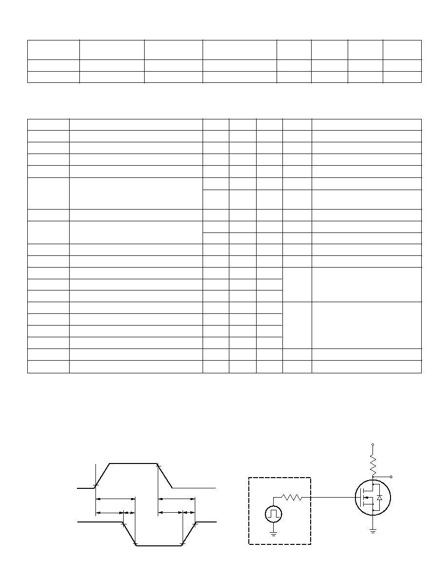
Switching Waveforms and Test Circuit
90%
10%
90%
90%
10%
10%
PULSE
GENERATOR
V
DD
R
L
OUTPUT
D.U.T.
t
(ON)
t
d(ON)
t
(OFF)
t
d(OFF)
t
F
t
r
INPUT
INPUT
OUTPUT
10V
V
DD
R
gen
0V
0V
Static Drain-to-Source
ON-State Resistance
TN2106
7-73
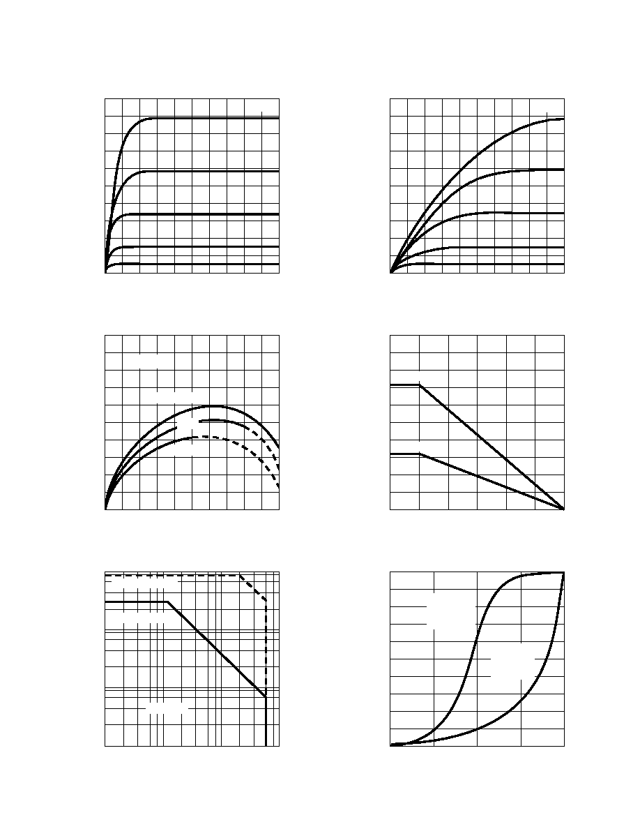
Typical Performance Curves
Output Characteristics
2.5
2.0
1.5
1.0
0.5
0
V
DS
(volts)
I
(amperes)
D
Saturation Characteristics
V
DS
(volts)
I
(amperes)
D
Maximum Rated Safe Operating Area
0.1
100
10
1
1.0
0.1
0.01
0.001
V
DS
(volts)
I
(amperes)
D
Thermal Response Characteristics
Thermal Resistance (normalized)
1.0
0.8
0.6
0.4
0.2
0
0.001
10
0.01
0.1
1.0
t
p
(seconds)
Transconductance vs. Drain Current
0.5
0.4
0.3
0.2
0.1
0
0
0.4
0.2
G
FS
(siemens)
I
D
(amperes)
Power Dissipation vs. Temperature
0
150
100
50
1.0
0.8
0.6
0.4
0.2
0
125
75
25
T
A
C)
∞
(
D
P
(watts)
TO-236AB
TA = 25
∞
C
PD = 0.36W
TO-92
SOT-23
T
A
= -55
∞
C
V
DS
= 25V
0
10
20
30
50
40
4V
3V
0
2
4
6
10
8
25
∞
C
125
∞
C
0.6
1.0
0.8
10V
8V
6V
2.5
2.0
1.5
1.0
0.5
0
4V
3V
10V
8V
6V
SOT-23 (DC)
SOT-23 (pulsed)
V
GS
=
V
GS
=
T
A
= 25
∞
C
TO-92
TC = 25
∞
C
PD = 1W
TN2106
7-74
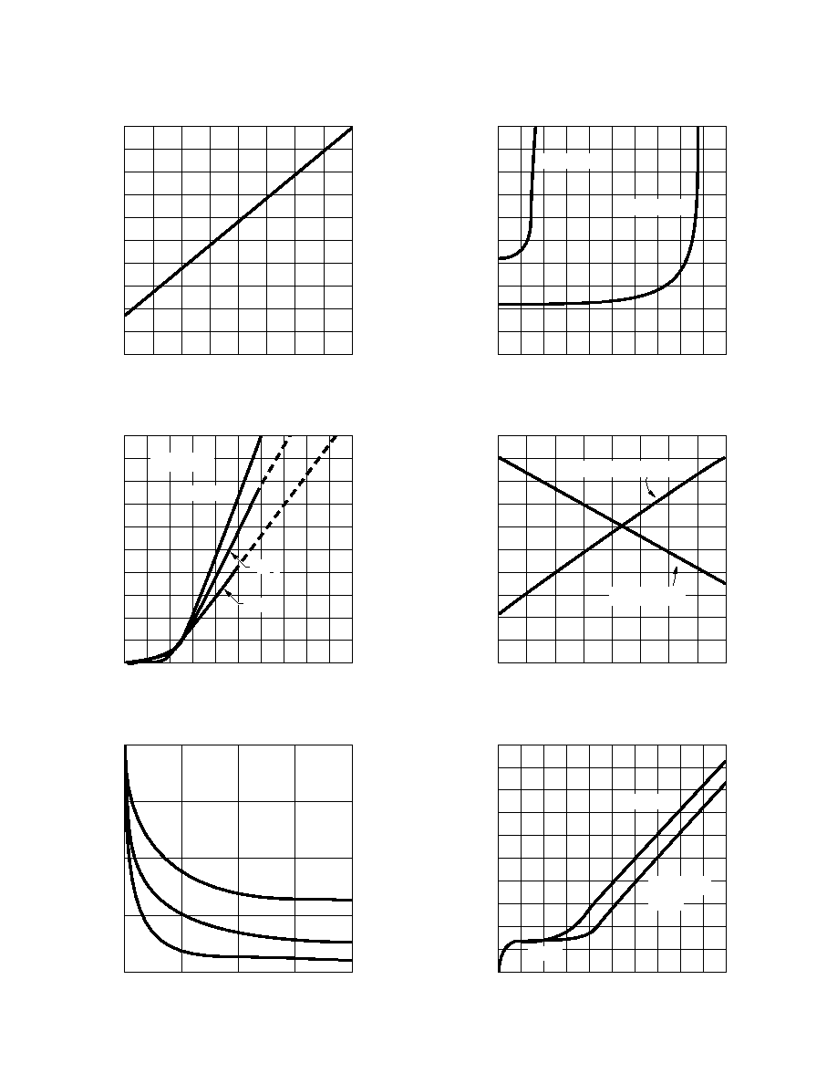
Typical Performance Curves
Gate Drive Dynamic Characteristics
Q
G
(nanocoulombs)
V
GS
(volts)
Tj (
∞
C)
V
GS(th)
(normalized)
R
DS(ON)
(normalized)
V
GS(th)
and R
DS(ON)
Variation with Temperature
On-Resistance vs. Drain Current
R
DS(ON)
(ohms)
BV
DSS
(normalized)
Tj (
∞
C)
Transfer Characteristics
V
GS
(volts)
I D
(amperes)
Capacitance vs. Drain-to-Source Voltage
100
C (picofarads)
V
DS
(volts)
ID (amperes)
BV
DSS
Variation with Temperature
0
10
20
30
40
50
75
25
0
0
2
4
6
8
10
1.0
0.8
0.6
0.4
0.2
0
-50
0
50
100
150
1.1
1.0
10
8
6
4
2
0
1.2
1.0
0.8
0.6
0.4
10
8
6
4
2
0
0.2
0.4
0.6
0.8
1.0
-50
0
50
100
150
38 pF
V
DS
= 20V
V
DS
= 10V
V
GS
= 4.5V
V
GS
= 10V
T
A
= -55
∞
C
V
DS
= 25V
125
∞
C
0
0.5
1.0
1.5
2.5
2.0
f = 1MHz
C
ISS
C
OSS
C
RSS
0.9
92 pF
2.0
1.6
1.2
0.8
0.4
0
V
GS(th)
@ 1mA
25
∞
C
0
R
DS(ON)
@ 10V, 0.5A
TN2106