
TP5322
Rev. 3 September 14, 2004
1
Initial Release
P-Channel Enhancement-Mode
Vertical DMOS FET
Features
!
Low threshold, -2.4V max.
!
High input impedance
!
Low input capacitance, 110pFmax.
!
Fast switching speeds
!
Low on resistance
!
Free from secondary breakdown
!
Low input and output leakage
!
Complementary N- and P-channel devices
Application
!
Logic level interfaces-ideal for TTL and CMOS
!
Battery operated systems
!
Photo voltaic devices
!
Analog switches
!
General purpose line drivers
!
Telecom switches
Absolute Maximum Ratings
Drain-to-Source Voltage
BV
DSS
Drain-to-Gate Voltage
BV
DGS
Gate-to-Source Voltage
±20V
Operating and Storage Temperature
-55∞C to +150∞C
Soldering Temperature****
300∞C
****Distance of 1.6mm from case for 10 seconds.
General Description
These low threshold enhancement-mode (normally-off)
transistors utilize an advanced vertical DMOS structure and
Supertex's well-proven silicon-gate manufacturing process. This
combination produces devices with the power handling
capabilities of bipolar transistors and with the high input
impedance and positive temperature coefficient inherent in MOS
devices. Characteristic of all MOS structures, these devices are
free from thermal runaway and thermally-induced secondary
breakdown.
Supertex's vertical DMOS FETs are ideally suited to a wide
range of switching and amplifying applications where very low
threshold voltage, high breakdown voltage, high input
impedance, low input capacitance, and fast switching speeds are
desired.
Package Options
Ordering Information
Order Number / Package
TO-243AA** TO-236AB***
BV
DSS
/
BV
DGS
R
DS(ON)
(max)
V
GS(th)
(max)
I
D(ON)
(min)
TP5322N8 TP5322K1
-220V
12
-2.4V -0.7A
TP5322N8-G* TP5322K1-G* -220V 12
-2.4V -0.7A
**Same as SOT-89. Product supplied on 2000 piece carrier tape reels.
***Same as SOT-23. Products supplied on 3000 piece carrier tape reels.
TP5322
A042005
* "Green" Certified Package
D
S
D
G
D
S
G
TO-236AB
(SOT-23)*
TO-243AA
(SOT-89)*
Product Marking for SOT-89
TP3C
Where
=2-week alpha date code
Product Marking for SOT-23
P3C
Where
=2-week alpha date code
TP5322
Rev. 3 September 14, 2004
2
Thermal Characteristics
Package I
D
(continuous)
I
D
(pulsed)
Power Dissipation @
T
A
= 25∞C
JC
∞C/W
JA
∞C/W
I
DR
* I
DRM
TO-243AA -0.26A -0.90A
1.6W
15 78**
-0.26A
-0.9A
TO-236AB -0.12A -0.70A
0.36W
200
350
-0.12A
-0.7A
*I
D
(continous) is limited by max rated Tj.
**Mounted on FR4 board, 25mm x 25mm x 1.57mm. Significant PD increase possible on ceramic substate.
Electrical Characteristics
(@25∞C unless otherwise specified)
Symbol Parameter
Min Typ Max Units Conditions
BV
DSS
Drain-to-Source
Breakdown Voltage
-220 V V
GS
= 0V, I
D
= -2mA
V
GS(th)
Gate Threshold Voltage
-1.0
-2.4
V
V
GS
= V
DS
, I
D
= -1mA
V
GS(th)
Change in V
GS(th)
with Temperature
4.5
mV/∞C V
GS
= V
DS
, I
D
= -1mA
I
GSS
Gate Body Leakage
-100
nA
V
GS
= ±20V, V
DS
= 0V
-10
µA
V
GS
= 0V, V
DS
= Max Rating
I
DSS
Zero Gate Voltage Drain Current
-1.0
mA
V
GS
= 0V, V
DS
= 0.8 Max
Rating, T
A
= 125∞C
I
D(ON)
On-State Drain Current
-0.7
-0.95
A
V
GS
= -10V, V
DS
= -25V
10 15
V
GS
= -4.5V, I
D
= -100mA
R
DS(ON)
Static
Drain-to-Source
ON-State Resistance
8.0 12
V
GS
= -10V, I
D
= -200mA
R
DS(ON)
Change in R
DS(ON)
with Temperature
1.7
%/∞C
V
GS
= -10V, I
D
= -200mA
G
FS
Forward
Transconductance
100 250 mmho
V
DS
= -25V, I
D
= -200mA
C
ISS
Input
Capacitance
110
C
OSS
Common Source Output Capacitance
45
C
RSS
Reverse Transfer Capacitance
20
pF
V
GS
= 0V, V
DS
= -25V
f = 1MHz
t
d(ON)
Turn-ON Delay Time
10
t
r
Rise
Time
15
t
d(OFF)
Turn-Off Delay Time
20
t
f
Fall
Time
15
ns
V
DD
= -25V,
I
D
= -0.7A
R
GEN
= 25
V
SD
Diode Forward Voltage Drop
-1.8
V
V
GS
= 0V, I
SD
= -0.5A
t
rr
Reverse Recovery Time
300
ns
V
GS
= 0V, I
SD
= -0.5A
Notes:
1) All DC parameters 100% tested at 25∞C unless otherwise stated. (Pulsed test: 300µs pulse at 2% duty cycle.)
2) All AC parameters sample tested.
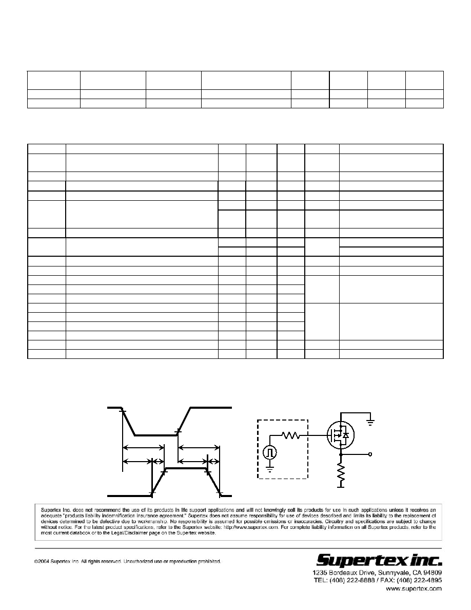
Switching Waveforms and Test Circuit
R
GEN
Input
Pulse
Generator
V
DD
R
L
D.U.T
OUTPUT
0V
-10V
0V
V
DD
t
d(OFF)
Input
Output
t
r
t
f
t
d(ON)
t
(ON)
t
(OFF)
Doc.# DSFP-TP5322 A042005