7-175
7
VN0645
VN0650
Order Number / Package
BV
DSS
/
R
DS(ON)
I
D(ON)
BV
DGS
(max)
(min)
TO-39
TO-92
Die
450V
16
0.5A
VN0645N2
--
--
500V
16
0.5A
--
VN0650N3
VN0650ND
MIL visual screening available
High Reliability Devices
See pages 5-4 and 5-5 for MILITARY STANDARD Process
Flows and Ordering Information.
Advanced DMOS Technology
The VN0650 is NOT recommended for new designs. Please
use VN2450 instead.
These enhancement-mode (normally-off) transistors utilize a
vertical DMOS structure and Supertex's well-proven silicon-gate
manufacturing process. This combination produces devices with
the power handling capabilities of bipolar transistors and with the
high input impedance and positive temperature coefficient inher-
ent in MOS devices. Characteristic of all MOS structures, these
devices are free from thermal runaway and thermally-induced
secondary breakdown.
Supertex's vertical DMOS FETs are ideally suited to a wide range
of switching and amplifying applications where high breakdown
voltage, high input impedance, low input capacitance, and fast
switching speeds are desired.
Package Options
Note: See Package Outline section for dimensions.
N-Channel Enhancement-Mode
Vertical DMOS FETs
TO-92
Features
s
Free from secondary breakdown
s
Low power drive requirement
s
Ease of paralleling
s
Low C
ISS
and fast switching speeds
s
Excellent thermal stability
s
Integral Source-Drain diode
s
High input impedance and high gain
s
Complementary N- and P-channel devices
Applications
s
Motor controls
s
Converters
s
Amplifiers
s
Switches
s
Power supply circuits
s
Drivers (relays, hammers, solenoids, lamps,
memories, displays, bipolar transistors, etc.)
Absolute Maximum Ratings
Drain-to-Source Voltage
BV
DSS
Drain-to-Gate Voltage
BV
DGS
Gate-to-Source Voltage
±
20V
Operating and Storage Temperature
-55
∞
C to +150
∞
C
Soldering Temperature*
300
∞
C
*
Distance of 1.6 mm from case for 10 seconds.
TO-39
Ordering Information
S G D
D G S
Case: DRAIN
7-176
VN0645/VN0650
Package
I
D
(continuous)*
I
D
(pulsed)
Power Dissipation
jc
ja
I
DR
*
I
DRM
@ T
C
= 25
∞
C
∞
C/W
∞
C/W
TO-39
0.4A
1.5A
6W
21
125
0.4A
1.5A
TO-92
0.2A
1.0A
1W
125
170
0.2A
1.0A
*
I
D
(continuous) is limited by max rated T
j
.
Thermal Characteristics
Symbol
Parameter
Min
Typ
Max
Unit
Conditions
BV
DSS
VN0650
500
VN0645
450
V
GS(th)
Gate Threshold Voltage
2
4
V
V
GS
= V
DS
, I
D
= 2mA
V
GS(th)
Change in V
GS(th)
with Temperature
-4.5
mV/
∞
C
V
GS
= V
DS
, I
D
= 2mA
I
GSS
Gate Body Leakage
100
nA
V
GS
=
±
20V, V
DS
= 0V
I
DSS
Zero Gate Voltage Drain Current
10
µ
A
V
GS
= 0V, V
DS
= Max Rating
1
mA
V
GS
= 0V, V
DS
= 0.8 Max Rating
T
A
= 125
∞
C
I
D(ON)
ON-State Drain Current
0.8
V
GS
= 5V, V
DS
= 25V
0.5
1.1
V
GS
= 10V, V
DS
= 25V
R
DS(ON)
12
V
GS
= 5V, I
D
= 100mA
11
16
V
GS
= 10V, I
D
= 400mA
R
DS(ON)
Change in R
DS(ON)
with Temperature
0.75
%/
∞
C
V
GS
= 10V, I
D
= 400mA
G
FS
Forward Transconductance
100
m
V
DS
= 25V, I
D
= 400mA
C
ISS
Input Capacitance
120
130
C
OSS
Common Source Output Capacitance
20
75
pF
C
RSS
Reverse Transfer Capacitance
10
20
t
d(ON)
Turn-ON Delay Time
10
t
r
Rise Time
10
t
d(OFF)
Turn-OFF Delay Time
20
t
f
Fall Time
10
V
SD
Diode Forward Voltage Drop
1.8
V
V
GS
= 0V, I
SD
= 0.4A
t
rr
Reverse Recovery Time
300
ns
V
GS
= 0V, I
SD
= 0.4A
Notes:
1. All D.C. parameters 100% tested at 25
∞
C unless otherwise stated. (Pulse test: 300
µ
s pulse, 2% duty cycle.)
2. All A.C. parameters sample tested.
Electrical Characteristics
(@ 25
∞
C unless otherwise specified)
Drain-to-Source
Breakdown Voltage
Static Drain-to-Source
ON-State Resistance
A
V
V
GS
= 0V, I
D
= 2mA
ns
V
GS
= 0V, V
DS
= 25V
f = 1 MHz
V
DD
= 25V,
I
D
= 0.5A,
R
GEN
= 25
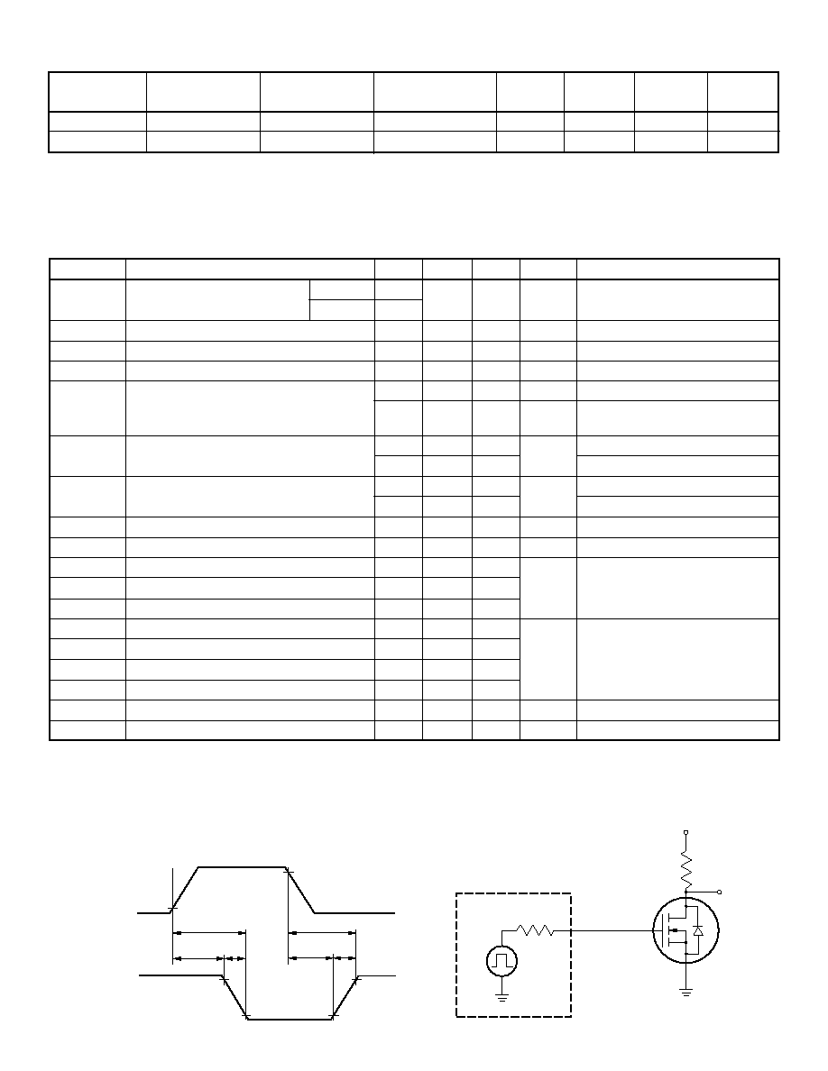
Switching Waveforms and Test Circuit
90%
10%
90%
90%
10%
10%
PULSE
GENERATOR
V
DD
R
L
OUTPUT
D.U.T.
t
(ON)
t
d(ON)
t
(OFF)
t
d(OFF)
t
F
t
r
INPUT
INPUT
OUTPUT
10V
V
DD
R
gen
0V
0V
7-177
7
VN0645/VN0650
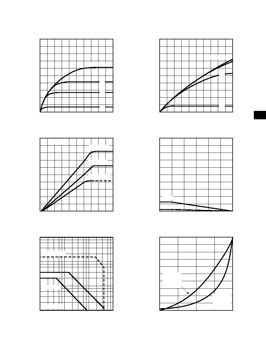
Typical Performance Curves
Output Characteristics
2.0
0
10
20
30
50
40
V
DS
(volts)
I
D
(amperes)
Saturation Characteristics
V
DS
(volts)
I
D
(amperes)
Maximum Rated Safe Operating Area
0.1
1.0
10
0.01
V
DS
(volts)
I
D
(amperes)
Thermal Response Characteristics
Thermal Resistance (normalized)
1.0
0.8
0.6
0.4
0.2
0.001
10
0.01
0.1
1
t
p
(seconds)
Transconductance vs. Drain Current
0.3
0.24
0.18
0.12
0.06
0
1.0
G
FS
(siemens)
I
D
(amperes)
Power Dissipation vs. Case Temperature
0
150
100
50
125
75
25
T
C
(
∞
C)
P
D
(watts)
1.0
1.0
0.5
0
2
4
6
10
8
50
40
30
20
10
TO-39
TO-92
T
A
= -55
∞
C
T
A
= 25
∞
C
T
A
= 150
∞
C
V
DS
= 25V
1
1000
100
10
TO-39 (DC)
TO-39
P
D
= 6W
T
C
= 25
∞
C
0
0.2
0.4
0.6
0.8
0
0
0
4V
VGS = 6V to 10V
3V
VGS = 6V to 10V
5V
0
4V
3V
TO-92 (DC)
TO-39 (pulsed)
TC = 25
∞
C
TO-92
P
D
= 1W
T
C
= 25
∞
C
7-178
VN0645/VN0650
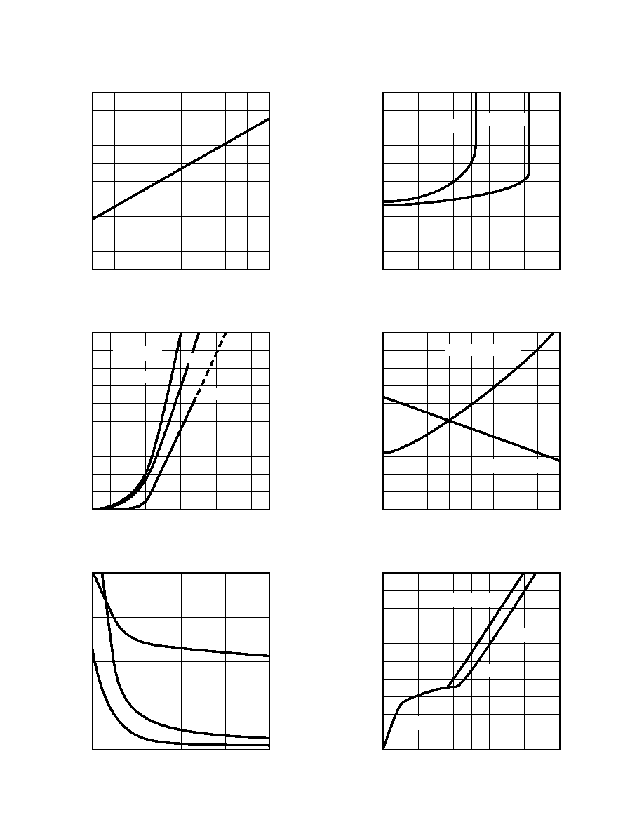
Typical Performance Curves
Gate Drive Dynamic Characteristics
Q
G
(nanocoulombs)
V
GS
(volts)
T
j
(
∞
C)
V
GS(th)
(normalized)
R
DS(ON)
(normalized)
V
(th)
and R
DS
Variation with Temperature
On-Resistance vs. Drain Current
R
DS(ON)
(ohms)
BV
DSS
(normalized)
T
j
(
∞
C)
Transfer Characteristics
V
GS
(volts)
Capacitance vs. Drain-to-Source Voltage
C (picofarads)
V
DS
(volts)
I
D
(amperes)
I
D
(amperes)
BV
DSS
Variation with Temperature
0
10
20
30
40
150
100
50
0
2
4
6
8
10
1.0
0.5
-50
0
50
100
150
1.1
1.0
0.9
30
12
1.4
1.2
1.0
0.8
0.6
10
8
6
4
2
0
0.5
1.0
1.5
2.0
2.5
-50
0
50
100
150
110 pF
V
DS
= 40V
V
DS
= 10V
179 pF
R
DS
@ 10V, 400mA
V
GS
= 5V
T
A
= -55
∞
C
V
DS
= 25V
f = 1MHz
C
ISS
C
OSS
C
RSS
25
∞
C
150
∞
C
0
0.3
0.6
0.9
1.5
1.2
6
18
24
V
(th)
@ 2mA
0
0
200
0
0
V
GS
= 10V
2.0
1.6
1.2
0.8
0.4
0