VN1206L/M, VN1210M
Siliconix
P-38211--Rev. C, 15-Aug-94
1
N-Channel Enhancement-Mode MOSFET Transistors
Product Summary
Part Number
V
(BR)DSS
Min (V)
r
DS(on)
Max (
W)
V
GS(th)
(V)
I
D
(A)
VN1206L
6 @ V
GS
= 10 V
0.8 to 2
0.23
VN1206M
120
6 @ V
GS
= 10 V
0.8 to 2
0.26
VN1210M
10 @ V
GS
= 2.5 V
0.8 to 2
0.2
Features
Benefits
Applications
D Low On-Resistance: 3.8 W
D Low Threshold: 1.4 V
D Low Input Capacitance: 35 pF
D Fast Switching Speed: 10 ns
D Low Input and Output Leakage
D Low Offset Voltage
D Low-Voltage Operation
D Easily Driven Without Buffer
D High-Speed Circuits
D Low Error Voltage
D Direct Logic-Level Interface: TTL/CMOS
D Drivers: Relays, Solenoids, Lamps, Hammers,
Displays, Memories, Transistors, etc.
D Battery Operated Systems
D Solid-State Relays
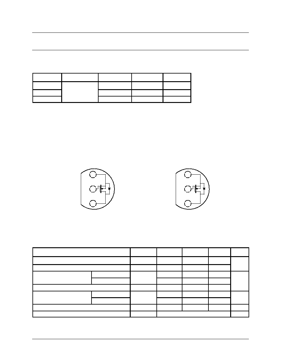
Top View
TO-226AA
(TO-92)
S
D
G
1
2
3
TO-237
(Tab Drain)
Top View
S
D
G
1
2
3
VN1206L
VN1206M
VN1210M
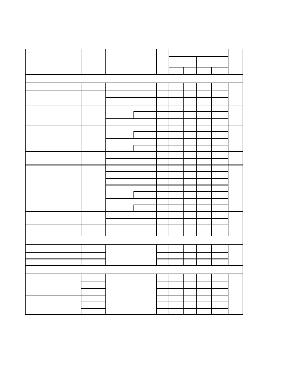
Absolute Maximum Ratings (T
A
= 25
_C Unless Otherwise Noted)
Parameter
Symbol
VN1206L
VN1206M
VN1210M
Unit
Drain-Source Voltage
V
DS
120
120
120
V
Gate-Source Voltage
V
GS
"30
"30
"30
V
Continuous Drain Current
T
A
= 25
_C
I
D
0.23
0.26
0.2
(T
J
= 150
_C)
T
A
= 100
_C
I
D
0.15
0.16
0.13
A
Pulsed Drain Current
a
I
DM
2
2
2
Power Dissipation
T
A
= 25
_C
P
D
0.8
1
1
W
Power Dissipation
T
A
= 100
_C
P
D
0.32
0.4
0.4
W
Maximum Junction-to-Ambient
R
thJA
156
125
125
_C/W
Operating Junction and Storage Temperature Range
T
J
, T
stg
�55 to 150
_C
Notes
a.
Pulse width limited by maximum junction temperature.
Updates to this data sheet may be obtained via facsimile by calling Siliconix FaxBack, 1-408-970-5600. Please request FaxBack document #70227.
VN1206L/M, VN1210M
2
Siliconix
P-38211--Rev. C, 15-Aug-94
Specifications
a
Limits
VN1206L
VN1206M
VN1210M
Parameter
Symbol
Test Conditions
Typ
b
Min
Max
Min
Max
Unit
Static
Drain-Source Breakdown Voltage
V
(BR)DSS
V
GS
= 0 V, I
D
= 100
mA
145
120
120
Gate Threshold Voltage
V
V
DS
= V
GS
, I
D
= 250
mA
1.4
V
Gate-Threshold Voltage
V
GS(th)
V
DS
= V
GS
, I
D
= 1 mA
1.5
0.8
2
0.8
2
V
DS
= 0 V, V
GS
=
"15 V
"100
"100
Gate-Body Leakage
I
GSS
T
J
= 125
_C
"500
"500
nA
V
DS
= 0 V, V
GS
=
"20 V
V
DS
= 96 V, V
GS
= 0 V
Zero Gate Voltage Drain Current
I
DSS
T
J
= 125
_C
mA
Zero Gate Voltage Drain Current
I
DSS
V
DS
= 120 V, V
GS
= 0 V
10
10
mA
T
J
= 125
_C
500
500
On State Drain Current
c
I
D(
)
V
DS
= 10 V, V
GS
= 4.5 V
0.6
A
On-State Drain Current
c
I
D(on)
V
DS
= 10 V, V
GS
= 10 V
1.6
1
1
A
V
GS
= 2.5 V, I
D
= 0.1 A
6
10
10
V
GS
= 3.5 V, I
D
= 0.1 A
4.5
V
GS
= 10 V, I
D
= 0.3 A
3.3
Drain-Source On-Resistance
c
r
DS(on)
V
GS
= 4.5 V, I
D
= 0.2 A
3.8
W
T
J
= 125
_C
7.6
V
GS
= 10 V, I
D
= 0.5 A
3.3
6
10
T
J
= 125
_C
7
14.8
24.7
Forward Transconductance
c
g
f
V
DS
= 10 V, I
D
= 0.2 A
400
Forward Transconductance
c
g
fs
V
DS
= 10 V, I
D
= 0.5 A
425
300
300
mS
Common Source
Output Conductance
c
g
os
V
DS
= 7.5 V, I
D
= 0.1 A
0.4
mS
Dynamic
Input Capacitance
C
iss
V
25 V V
0 V
35
125
125
Output Capacitance
C
oss
V
DS
= 25 V, V
GS
= 0 V
f = 1 MHz
15
50
50
pF
Reverse Transfer Capacitance
C
rss
2
20
20
Switching
d
t
ON
6
Turn-On Time
t
d(on)
3
8
8
t
r
V
DD
= 60 V, R
L
= 150 W
I
D
^ 0 4 A V
GEN
= 10 V
3
8
8
ns
t
OFF
I
D
^ 0.4 A, V
GEN
= 10 V
R
G
= 25 W
10
ns
Turn-Off Time
t
d(off)
7
18
18
t
f
2.5
12
12
Notes
a.
T
A
= 25
_C unless otherwise noted.
VNDQ12
b.
For DESIGN AID ONLY, not subject to production testing.
c.
Pulse test: PW
v300 ms duty cycle v2%.
d.
Switching time is essentially independent of operating temperature.
VN1206L/M, VN1210M
Siliconix
P-38211--Rev. C, 15-Aug-94
3
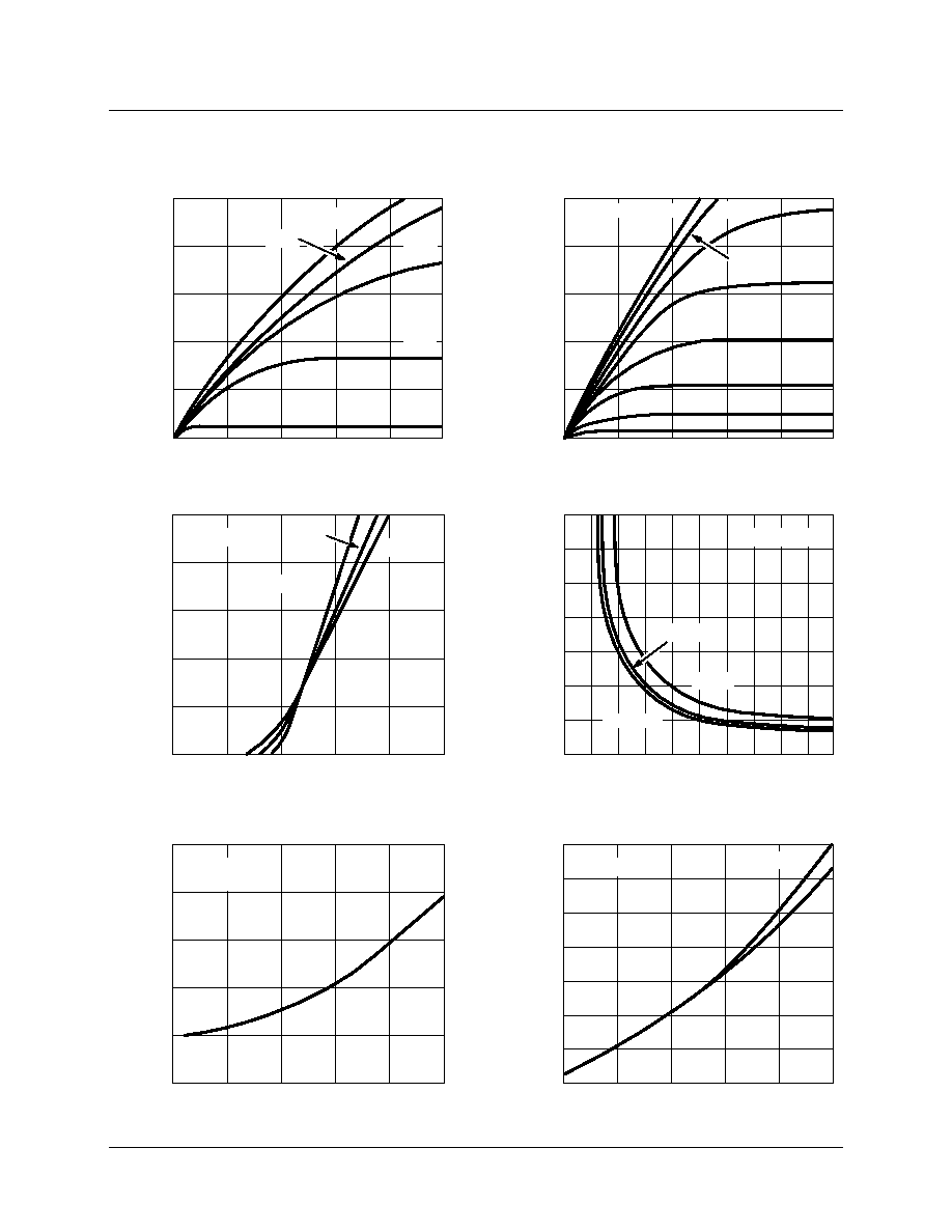
Typical Characteristics (25
_C Unless Otherwise Noted)
Ohmic Region Characteristics
Output Characteristics for Low Gate Drive
On-Resistance vs. Drain Current
Normalized On-Resistance
vs. Junction Temperature
Transfer Characteristics
On-Resistance vs. Gate-to-Source Voltage
V
GS
� Gate-Source Voltage (V)
V
GS
� Gate-Source Voltage (V)
� Drain Current (mA)
I
D
� Drain Current (mA)
I
D
� Drain Current (mA)
I
D
� On-Resistance (
r
DS(on)
V
DS
� Drain-to-Source Voltage (V)
V
DS
� Drain-to-Source Voltage (V)
I
D
� Drain Current (A)
T
J
� Junction Temperature (
_C)
r
DS(on)
� Drain-Source On-Resistance
(Normalized)
1000
0
1
2
3
4
5
800
600
400
200
0
6 V
4 V
3 V
2 V
V
GS
= 10 V
200
0
0.4
0.8
1.2
1.6
2.0
160
120
80
40
0
V
GS
= 3.0 V
2.6 V
2.4 V
2.2 V
2.0 V
1.8 V
1.6 V
2.8 V
500
400
300
0
0
1
5
200
100
2
3
4
125
_C
25
_C
T
J
= �55
_C
5.0
4.5
4.0
2.5
0
0.2
1.0
3.5
3.0
0.4
0.6
0.8
V
GS
= 10 V
T
J
= 25
_C
6.0
0
20
5.5
5.0
4.5
2.5
4.0
3.5
3.0
10
I
D
= 0.1 A
0.5 A
0.25 A
T
J
= 25
_C
2.25
2.00
1.75
0.50
�50
�10
150
1.50
1.25
30
70
110
1.00
0.75
0.1 A
I
D
= 0.5 A
V
GS
= 10 V
V
DS
= 10 V
r
DS(on)
� Drain-Source On-Resistance (
W
)
W
)
VN1206L/M, VN1210M
4
Siliconix
P-38211--Rev. C, 15-Aug-94
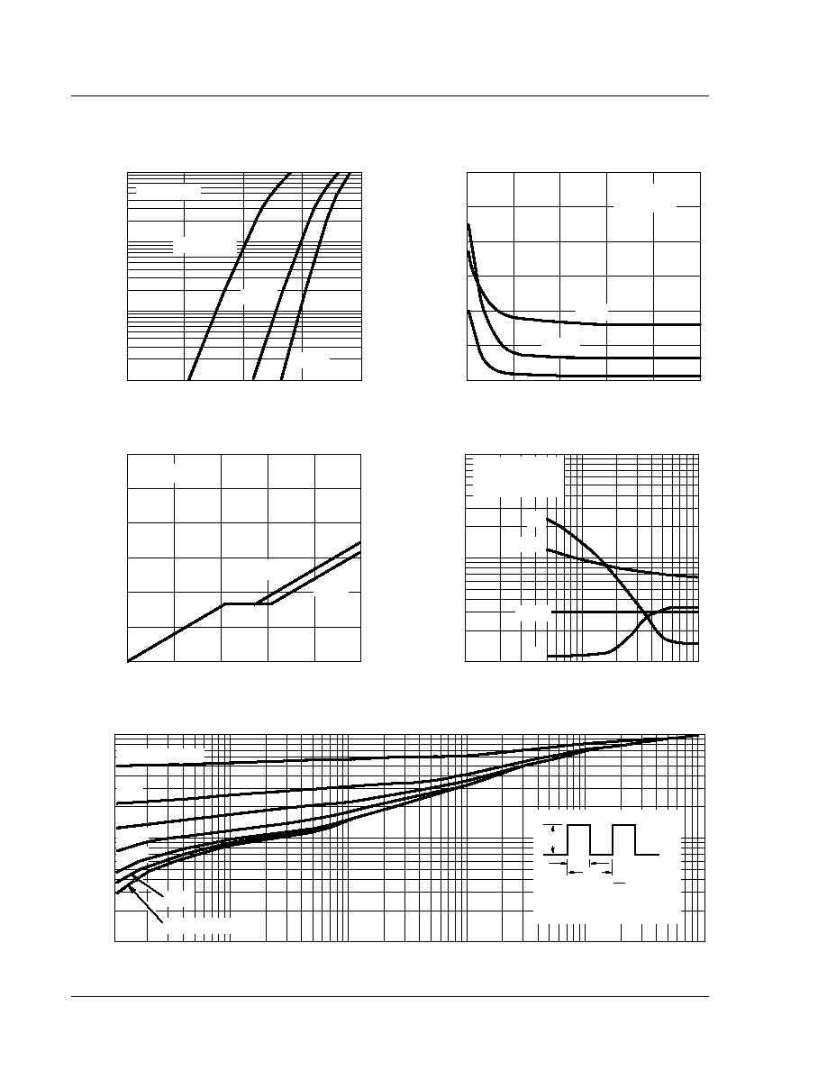
Typical Characteristics (25
_C Unless Otherwise Noted) (Cont'd)
10
100
1000
100
10
1
V
DD
= 25 V
R
G
= 25
W
V
GS
= 0 to 10 V
10 K
Duty Cycle = 0.5
0.2
0.1
0.05
0.02
Single Pulse
1
0.01
0.1
0.01
0.1
1
100
10
1 K
Threshold Region
Capacitance
Normalized Effective Transient Thermal Impedance, Junction-to-Ambient (TO-226AA)
Gate Charge
Load Condition Effects on Switching
Normalized Ef
fective
T
ransient
Thermal Impedance
t
1
� Square Wave Pulse Duration (sec)
I
D
� Drain Current (A)
V
DS
� Drain-to-Source Voltage (V)
V
GS
� Gate-to-Source Voltage (V)
Q
g
� Total Gate Charge (pC)
� Drain Current (mA)
I
D
C � Capacitance (pF)
� Gate-to-Source
V
oltage (V)
V
GS
t � Switching
T
ime (ns)
t
d(on)
t
d(off)
t
r
t
f
1. Duty Cycle, D =
2. Per Unit Base = R
thJA
= 156
_
C/W
3. T
JM
� T
A
= P
DM
Z
thJA
(t)
t
1
t
2
t
1
Notes:
P
DM
t
2
10
1
0.01
0
0.5
0.1
1
1.5
2
�55
_C
25
_C
T
J
= 150
_C
120
100
80
0
0
10
50
60
40
20
30
40
20
C
rss
C
iss
C
oss
12
10
8
0
0
120
600
6
4
240
360
480
2
96 V
I
D
= 0.5 A
V
DS
= 60 V
V
DS
= 15 V
V
GS
= 0 V
f = 1 MHz