
Features
- High gain bandwidth product
f
T
= 7 GHz
- High power gain
|S
21
|
2
= 7 dB @ V
CE
= 5 V, I
C
= 100 mA, f = 1 GHz
- High power
P
OUT
= 32 dBm (1.5 W) @ V
CE
= 6 V, I
CQ
= 5 mA, f = 465 MHz
Applications
- UHF and VHF wide band amplifier
Page 1 of 7
http://www.tachyonics.co.kr
July 2005.
Rev. 1.0
NPN SiGe RF TRANSISTOR
Specification
THN6601B
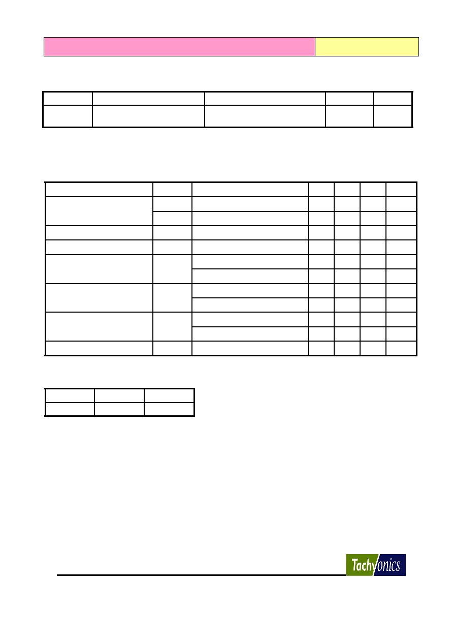
Absolute Maximum Ratings (T
A
= 25
)
PIN CONFIGURATION
1. Emitter
2. Base
3. Emitter
4. Collector
Collector to Base Breakdown Voltage
Collector to Emitter Breakdown Voltage
Emitter to Base Breakdown Voltage
Collector Current
Total Power Dissipation
Junction Temperature
Storage Temperature
150
I
C
500
mA
W
Unit
BV
CBO
20
V
Parameter
Symbol
P
tot
1.5
Ratings
T
stg
-65 ~ 150
V
BV
EBO
3
V
BV
CEO
12
T
j
SOT223
Unit in mm
6.5
7.
0
3.0
3.
5
1
2
3
4
2.3
4.6
0.7
Electrical Characteristics (T
A
= 25
)
Page 2 of 7
http://www.tachyonics.co.kr
July 2005.
Rev. 1.0
Specification
THN6601B
dB
12
9
V
CE
= 7 V, I
C
= 100 mA, f = 1 GHz
dB
11
8
V
CE
= 5 V, I
C
= 100 mA, f = 1 GHz
MAG
Maximum Available Gain
dB
7
5
V
CE
= 5 V, I
C
= 100 mA, f = 1 GHz
|S
21
|
2
Insertion Power Gain
GHz
7.0
5
V
CE
= 7 V, I
C
= 100 mA
300
50
V
CE
= 5 V, I
C
= 100 mA
h
FE
DC Current Gain
GHz
6
4
V
CE
= 5 V, I
C
= 100 mA
f
T
Gain Bandwidth Product
dB
7
5
V
CE
= 7 V, I
C
= 100 mA, f = 1 GHz
0.5
V
CB
= 19 V, I
E
= 0 mA
I
CBO
Collector Cut-off Current
10
V
CE
= 12 V, I
B
= 0 mA
I
CEO
0.5
V
EB
= 1.5 V, I
C
= 0 mA
I
EBO
Emitter Cut-off Current
1.9
Typ.
Max.
pF
V
CB
= 6 V, I
E
= 0 mA, f = 1 MHz
C
re
Reverse Transfer Capacitance
Unit
Min.
Test Conditions
Symbol
Parameter
h
FE
Classification
170 - 300
50 - 200
h
FE
Value
R1601
�
R1601
Marking
Thermal Characteristics
K/W
55
P
tot
= 1.5 W; T
S
= 60
; note 1
Thermal resistance from junction
to soldering point
R
th
j-s
Unit
Value
Condition
Parameter
Symbol
Note 1. T
S
is the temperature at the soldering point of the collector pin.

Typical Characteristics ( T
A
= 25
, unless otherwise specified)
Page 3 of 7
http://www.tachyonics.co.kr
July 2005.
Rev. 1.0
Specification
THN6601B
Power Dissipation
vs. Ambient Temperature
DC Current Gain
vs. Collector Current
Collector Current
vs. Base to Emitter Voltage
Reverse Transfer Capacitance
vs. Collector to Base Voltage
0
25
50
75
100
125
150
0.0
0.5
1.0
1.5
2.0
Co
l
l
e
c
t
or
Po
wer
Di
s
s
i
pa
t
i
on
,
P
tot
(W
)
Ambient Temperature, T
A
(
o
C)
0.0 0.1 0.2 0.3 0.4 0.5 0.6 0.7 0.8 0.9 1.0
0
5
10
15
20
25
30
V
CE
= 5 V
C
o
llector Cu
rren
t
,
I
C
(m
A)
Base to Emitter Voltage, V
BE
(V)
0
2
4
6
8
10
1.0
1.5
2.0
2.5
3.0
3.5
4.0
Revers
e T
r
ans
f
e
r C
a
pac
it
an
c
e
,
C
re
(p
F
)
Collector to Base Voltage, V
CB
(V)
10
-3
10
-2
10
-1
10
0
0
20
40
60
80
100
120
140
160
V
CE
= 5 V
DC
Cu
rr
e
n
t
G
a
i
n
,
h
FE
Collector Current, I
C
(A)

Page 4 of 7
http://www.tachyonics.co.kr
July 2005.
Rev. 1.0
Specification
THN6601B
Collector Current
vs. Collector to Emitter Voltage
Gain Bandwidth Product
vs. Collector Current
Insertion Power Gain
vs. Collector Current
10
100
1000
0
2
4
6
8
10
12
Ins
e
rtion
Pow
e
r Gain, |
S
21
|
2
(dB)
Collector Current, I
C
(mA)
V
CE
= 5 V
V
CE
= 7 V
f = 1 GHz
10
100
1000
0
2
4
6
8
10
12
14
16
18
20
M
a
x
i
mu
m A
v
a
i
l
a
b
l
e
G
a
i
n
,
M
A
G
(
d
B
)
Collector Current, I
C
(mA)
V
CE
= 5 V
V
CE
= 7 V
f = 1 GHz
Maximum Available Gain
vs. Collector Current
10
100
1000
0
2
4
6
8
10
Ga
in Bandwid
t
h
Prod
uct
,
f
T
(GH
z
)
Collector Current, I
C
(mA)
V
CE
= 5 V
V
CE
= 7 V
0
1
2
3
4
5
6
7
8
9 10
0.0
0.1
0.2
0.3
0.4
0.5
0.6
0.7
I
B
step = 1.8 m A
C
o
llec
tor Current,
I
C
(A)
Collector to Em itter Voltage, V
CE
(V)

Page 5 of 7
http://www.tachyonics.co.kr
July 2005.
Rev. 1.0
Specification
THN6601B
Output Power or Power Gain
vs. Input Power
30
P
OUT
(dBm)
56
11
6
465
CW, class-AB
C
(%)
G
P
(dB)
V
CE
(V)
f (MHz)
Operation Mode
Power Gain or Collector Efficiency
vs. Output Power
Application Information
RF performance at T
S
60
in common emitter configuration
0
5
10
15
20
25
30
0
5
10
15
20
25
30
35
40
0
2
4
6
8
10
12
14
16
18
f = 465 MHz, V
CE
= 6 V, I
CQ
= 5 mA
P
OUT
G
P
Out
put Pow
e
r,
P
OU
T
(dBm
)
Input Power, P
IN
(dBm)
Pow
e
r G
a
in, G
P
(dB)
10
15
20
25
30
35
0
2
4
6
8
10
12
14
16
18
20
0
10
20
30
40
50
60
70
80
90
100
C
G
P
f = 465 MHz, V
CE
= 6 V, I
CQ
= 4 mA
Power Gain,
G
P
(dB)
Output Power, P
OUT
(dBm)
C
o
ll
e
c
to
r E
f
f
i
ci
e
n
cy
,
C
(%)