Dimensions: Inches (Millimeters)
Tolerance: ±0.010 (0.25) unless specified otherwise
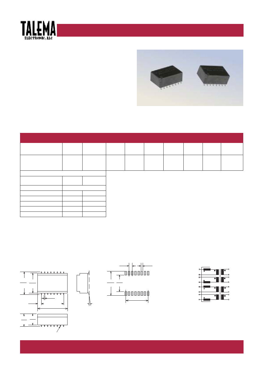
MUJ Series S
O
3kV Interface Transformer Modules
0
5
9
0
6
N
E
l
e
v
e
L
n
o
i
t
a
l
u
s
n
I
d
e
c
r
o
f
n
i
e
R
h
t
i
w
y
l
p
m
o
c
s
e
l
u
d
o
M
V
K
3
r
e
b
m
u
N
t
r
a
P
L
P
)
n
i
M
H
m
(
o
i
t
a
R
s
n
r
u
T
%
1
±
L
L
)
x
a
M
H
µ
(
^
I
C
D
)
A
m
(
C
C
)
x
a
M
F
p
(
R
U
C
P
)
s
m
h
O
(
R
U
C
S
)
s
m
h
O
(
V
P
)
s
m
r
V
(
c
i
t
a
m
e
h
c
S
X
X
X
-
1
B
0
0
2
-
J
U
M
0
3
:
1
:
1
1
:
1
0
1
4
5
7
7
.
1
9
.
1
0
0
0
3
A
X
X
X
-
1
B
0
4
2
-
J
U
M
0
3
:
1
:
1
2
:
2
0
1
4
5
7
7
.
1
7
.
3
0
0
0
3
A
X
X
X
-
1
B
0
3
2
-
J
U
M
0
3
:
1
:
1
5
.
2
:
5
.
2
0
1
4
5
7
7
.
1
4
.
4
0
0
0
3
A
e
k
o
h
C
d
a
u
Q
e
d
o
M
n
o
m
m
o
C
x
if
f
u
S
+
N
/
P
c
i
s
a
B
2
0
5
-
1
B
0
4
2
-
J
U
M
:
e
l
p
m
a
x
E
(
L
N
)
H
µ
(
R
U
C
)
s
m
h
O
(
0
0
0
-
e
k
o
h
C
o
N
0
7
4
-
7
4
4
.
0
1
0
1
-
0
0
1
6
.
0
1
0
5
-
0
0
5
4
.
0
2
0
5
-
0
0
0
5
1
.
1
3
2
1
-
0
0
0
2
1
8
.
1
Electrical Specifications @ 25∞C
Turns Ratio: Bold = IC side windings
Features
∑ excellent output characteristics ensure compliance with CCITT.I.430
pulse waveform template when used with recommended IC pairing
∑ SMD modules are designed for pick and place compatability
∑ excellent and consistent balance between windings
∑ modular design maximizes suppression effectivity and transmission
properties
∑ compact module eliminates three components reducing assembly and
storage cost
∑ full compatibility with all common IC's
∑ operating temperature:-40∞C to +85∞C
storage temperature: -40∞C to +125∞C
Standard Packaging: Tape and Reel
(01-03) Communications\MHJ
Suggested Pad Layout
Schematic
Test Conditions:
S
O
Transformer modules comply with Reinforced Insulation Level EN60950:1992/A4:
1997, para. 2.9.4.4 when tested in accordance with 6.4.1
1. Polarity and Turns Ratio: w1 : w2 : w3 : w4 ±1%
2. Inductance: 30mH Minimum, line side windings (w3+w4) in series @ 10kHz, 100mV
3. Leakage Inductance: 10µH Max. @ 100kHz, 100mV
4. Quad Choke Inductance: 100kHz, 20mV
5. Winding Capacitance: C
W
150pF Max. (w3+w4)
6. Coupling Capacitance: C
C
75pF Max. (w3+w4 to w1+w2) @ 10kHz, 100mV
7. High Voltage Test: 4kV, 1 minute U(w3+w4 to w1+w2)
High Voltage Pulse Test: U
PULSE
(w3+w4 to w1+w2); 10kV
OP
for 1,2µs/50µs wave form
U
PULSE
(w3+w4 to w1+w2); 10kV
OP
for 10µs/700µs wave form
MHJ Module
0∞ - 8∞
Surface Coplanarity will be 0.004(0.10) maximum
0.059
(1.50)
0.100
(2.54)
0.756
(19.2)
0.520
(13.2)
0.700
(17.78)
IC
Line
16
15
14
13
12
11
10
9
1
2
3
4
5
6
7
8
W1
W1
W2
W2
W3
W3
W4
W4
Pins - 0.012 x 0.020 (0.3 x 0.5)
0.394
(10.0)
0.346
(8.8)
0.945
(24.00)
0.717
(18.2)
0.122
(3.11)
0.630
(16.0)
7 x 0.100 (2,54)
0.020
(0.50)
TALEMA IN
WK/YR
Part Number
Talema Electronic ∑ 101 West 10th Street ∑ Rolla, MO (573) 364-2422 ∑ Fax: (573) 364-5390
www.talema.com ∑ Email: sales@talema.com