Features
∑ EMI noise suppression in the common mode
∑ small size SMD package for high density board placement
∑ SMD package is pick and place compatible and provides
consistent and reliable coplanarity
∑ low leakage inductance
∑ excellent quality at extremely competitive price due to high
volume production
∑ manufactured in ISO-9001 approved Talema facility
Typical Applications include: General Isolation, Telecommunications,
LAN Coupling and Isolation, Modems, Voltage Step-Up or Step-Down,
Impedance Matching and Baluns
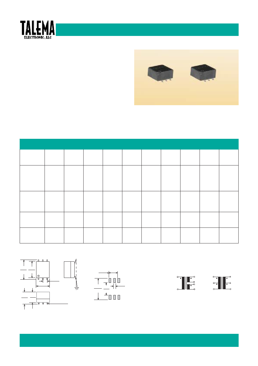
TGJ
TGJ Series ∑ General Purpose Coupling Transformers
Dimensions: Inches (Millimeters)
Tolerance: ±0.010 (0.25) unless specified otherwise
Surface coplanarity will be 0.004 (0.01)
Electrical Specifications
Ratings@ 25∞C ambient
Power Rating with 40∞C temperature rise : 500mW
Dielectric Strength between windings: 500Vrms
Operating Temperature Range: 0 to +70∞C
Storage Temperature: -25∞C to +105∞C
Insulation Resistance: 10,000 MOhm minimum
Test Frequency: Inductance measured @ 100kHz/20mVrms
s
e
k
o
h
C
n
o
i
s
s
e
r
p
p
u
S
e
s
i
o
N
I
M
E
e
d
o
M
n
o
m
m
o
C
D
M
S
∑
s
e
i
r
e
S
J
G
T
r
e
b
m
u
N
t
r
a
P
L
C
O
)
%
0
3
±
H
µ
(
s
n
r
u
T
o
i
t
a
R
%
2
±
L
L
c
e
S
/i
r
P
)
x
a
M
H
µ
(
C
C
c
e
S
/i
r
P
)
x
a
M
F
p
(
e
s
i
R
e
m
i
T
)
x
a
M
S
n
(
y
r
a
m
i
r
P
T
E
)
n
i
M
S
µ
-
V
(
R
U
C
P
)
s
m
h
O
m
(
R
U
C
S
)
s
m
h
O
m
(
R
U
C
T
)
s
m
h
O
m
(
c
i
t
a
m
e
h
c
S
C
6
-
0
5
-
J
G
T
0
5
1
:
1
:
1
5
.
0
8
1
6
.
5
2
.
5
0
1
1
0
1
1
0
2
1
C
C
6
-
0
0
2
-
J
G
T
0
0
2
1
:
1
:
1
3
.
0
8
1
2
.
4
9
.
5
0
1
2
0
1
2
0
4
2
C
C
6
-
0
0
5
-
J
G
T
0
0
5
1
:
1
:
1
4
.
0
2
3
3
.
5
5
.
8
0
3
3
0
3
3
0
9
3
C
C
6
-
0
0
0
2
-
J
G
T
0
0
0
2
1
:
1
:
1
8
.
0
7
3
2
.
8
6
1
0
9
6
0
9
6
0
1
8
C
C
6
-
0
0
0
5
-
J
G
T
0
0
0
5
1
:
1
:
1
3
.
1
0
6
5
.
0
1
5
2
0
7
3
1
0
7
3
1
0
3
1
C
G
6
-
0
0
2
-
J
G
T
0
0
2
1
:
1
:
2
8
.
0
8
2
.
3
0
.
5
0
1
2
5
0
1
5
0
1
G
G
6
-
0
0
5
-
J
G
T
0
0
5
1
:
1
:
2
1
.
1
1
1
6
.
5
5
.
8
0
3
3
5
6
1
5
6
1
G
G
6
-
0
0
0
2
-
J
G
T
0
0
0
2
1
:
1
:
2
8
.
1
9
1
1
1
6
1
0
9
6
5
4
3
5
4
3
G
G
6
-
0
0
0
5
-
J
G
T
0
0
0
5
1
:
1
:
2
6
.
3
3
3
6
1
5
2
0
0
1
1
0
5
5
0
5
5
G
D
6
-
0
0
2
-
J
G
T
0
0
2
t
c
1
:t
c
1
3
.
0
8
1
2
.
4
0
.
5
0
1
2
0
1
2
-
-
D
D
6
-
0
0
5
-
J
G
T
0
0
5
t
c
1
:t
c
1
4
.
0
2
3
3
.
5
5
.
8
0
0
3
0
3
3
-
-
D
D
6
-
0
0
0
2
-
J
G
T
0
0
0
2
t
c
1
:t
c
1
8
.
0
7
3
2
.
8
6
1
0
9
6
0
9
6
-
-
D
H
G
-
0
0
2
-
J
G
T
0
0
2
t
c
1
:t
c
2
8
.
0
8
2
.
3
0
.
5
0
0
3
0
5
1
-
-
H
H
6
-
0
0
5
-
J
G
T
0
0
5
t
c
1
:t
c
2
2
.
1
2
1
6
.
5
5
.
8
0
3
3
5
6
1
-
-
H
H
6
-
0
0
0
2
-
J
G
T
0
0
0
2
t
c
1
:t
c
2
8
.
1
9
1
1
1
6
1
0
9
6
5
4
3
-
-
H
0.283
(7.20)
0.244
(6.20)
0.020 x 0.12
(0.50 x 0.30)
0.100
(2.54)
0.374
(9.50)
0.453
(11.50)
TALEMA IN
WK/YR
Part Number
0.307
(7.80)
0∞ - 8∞
Suggested Pad
Layout
0.287
(7.30)
0.047
(1.20)
0.200
(5.08)
0.492
(12.50)
Schematic
1
2
3
D & H
6
5
4
2
5
3
4
1
6
C & G
Talema Electronic ∑ 101 West 10th Street ∑ Rolla, MO (573) 364-2422 ∑ Fax: (573) 364-5390
www.talema.com ∑ Email: sales@talema.com