 | –≠–ª–µ–∫—Ç—Ä–æ–Ω–Ω—ã–π –∫–æ–º–ø–æ–Ω–µ–Ω—Ç: TSL1301 | –°–∫–∞—á–∞—Ç—å:  PDF PDF  ZIP ZIP |
TSL1301
102
◊
1 LINEAR SENSOR ARRAY WITH HOLD
TAOS006B ≠ JUNE 2001
1
www.taosinc.com
t
t
Copyright
E
2001, TAOS Inc.
D
102
◊
1 Sensor-Element Organization
D
300 Dots-Per-Inch (DPI) Sensor Pitch
D
High Sensitivity
D
Output Referenced to Ground
D
Excellent High-Temperature Dark Signal
Characteristics
D
Operation to 2 MHz
D
Single 5-V Supply
Description
The TSL1301 linear sensor array consists of a 102
◊
1 array of photodiodes, associated charge amplifier
circuitry, and a pixel data-hold function that provides simultaneous-integration start and stop times for all pixels.
The pixels measure 85
µ
m by 77
µ
m with 85-
µ
m center-to-center spacing and 8-
µ
m spacing between pixels.
Operation is simplified by internal control logic that requires only a serial-input (SI) signal and a clock.
The TSL1301 is intended for use in a wide variety of applications including mark and code reading, OCR and
contact imaging, edge detection and positioning, and optical encoding.
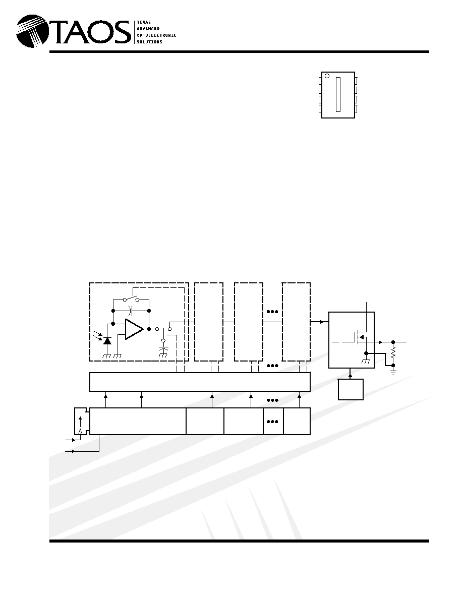
Functional Block Diagram
1
2
SI
CLK
102-Bit Shift Register
Q102
Switch Control Logic
Integrator
Reset
_
+
Pixel 1
Pixel
2
Pixel
102
Pixel
3
Sample/
Output
Analog
Bus
Output
Amplifier
6,7
Gain
Trim
Q3
Q2
Q1
V
DD
4
3
R
L
(External
Load)
AO
Hold
t
t
Texas Advanced Optoelectronic Solutions Inc.
800 Jupiter Road, Suite 205
S
Plano, TX 75074
S
(972) 673-0759
1
2
3
4
8
7
6
5
SI
CLK
AO
V
DD
NC
GND
GND
NC
(TOP VIEW)
NC ≠ No internal connection
TSL1301
102
◊
1 LINEAR SENSOR ARRAY WITH HOLD
TAOS006B ≠ JUNE 2001
2
www.taosinc.com
t
t
Copyright
E
2001, TAOS Inc.
Terminal Functions
TERMINAL
DESCRIPTION
NAME
NO.
DESCRIPTION
AO
3
Analog output
CLK
2
Clock. The clock controls charge transfer, pixel output, and reset.
GND
6, 7
Ground (substrate). All voltages are referenced to the substrate.
NC
5, 8
No internal connection
SI
1
Serial input. SI defines the start of the data-out sequence.
V
DD
4
Supply voltage. Supply voltage for both analog and digital circuits.
Detailed Description
The sensor consists of 102 photodiodes arranged in a linear array. Light energy impinging on a photodiode
generates photocurrent, which is integrated by the active integration circuitry associated with that pixel.
During the integration period, a sampling capacitor connects to the output of the integrator through an analog
switch. The amount of charge accumulated at each pixel is directly proportional to the light intensity and the
integration time.
The output and reset of the integrators is controlled by a 102-bit shift register and reset logic. An output cycle
is initiated by clocking in a logic 1 on SI. An internal signal, called Hold, is generated from the rising edge of SI
and transmitted to analog switches in the pixel circuit. This causes all 102 sampling capacitors to be
disconnected from their respective integrators and starts an integrator reset period. As the SI pulse is clocked
through the shift register, the charge stored on the sampling capacitors is sequentially connected to a
charge-coupled output amplifier that generates a voltage on analog output AO. Simultaneously, during the first
18 clock cycles, all pixel integrators are reset, and the next integration cycle begins on the 19th clock. On the
103rd clock rising edge, the SI pulse is clocked out of the shift register and the analog output AO assumes a
high impedance state. Note that this 103rd clock pulse is required to terminate the output of the 102nd pixel,
and return the internal logic to a known state. A subsequent SI pulse may be presented as early as the 104th
clock pulse, thereby initiating another pixel output cycle.
AO is driven by a source follower that requires an external pulldown resistor. When the output is not in the output
phase, it is in a high-impedance state. The output is nominally 0 V for no light input and 2 V for a nominal
white-level output, with a nominal full-scale (saturation) voltage of 3 V.
The TSL1301 is intended for use in a wide variety of applications, including: image scanning, mark and code
reading, optical character recognition (OCR) and contact imaging, edge detection and positioning, and optical
linear and rotary encoding.
TSL1301
102
◊
1 LINEAR SENSOR ARRAY WITH HOLD
TAOS006B ≠ JUNE 2001
3
www.taosinc.com
t
t
Copyright
E
2001, TAOS Inc.
Absolute Maximum Ratings
Supply voltage, V
DD
7 V
. . . . . . . . . . . . . . . . . . . . . . . . . . . . . . . . . . . . . . . . . . . . . . . . . . . . . . . . . . . . . . . . . . . . . . . .
Digital input current range, I
I
≠20 mA to 20 mA
. . . . . . . . . . . . . . . . . . . . . . . . . . . . . . . . . . . . . . . . . . . . . . . . . . . . .
Operating free-air temperature range, T
A
0
∞
C to 70
∞
C
. . . . . . . . . . . . . . . . . . . . . . . . . . . . . . . . . . . . . . . . . . . . . .
Storage temperature range, T
stg
≠25
∞
C to 85
∞
C
. . . . . . . . . . . . . . . . . . . . . . . . . . . . . . . . . . . . . . . . . . . . . . . . . . . .
Lead temperature 1,6 mm (1/16 inch) from case for 10 seconds
260
∞
C
. . . . . . . . . . . . . . . . . . . . . . . . . . . . . . .
Stresses beyond those listed under "absolute maximum ratings" may cause permanent damage to the device. These are stress ratings only, and
functional operation of the device at these or any other conditions beyond those indicated under "recommended operating conditions" is not
implied. Exposure to absolute-maximum-rated conditions for extended periods may affect device reliability.
Recommended Operating Conditions (see Figure 1 and Figure 2)
MIN
NOM
MAX
UNIT
Supply voltage, V
DD
4.5
5
5.5
V
Input voltage, V
I
0
V
DD
V
High-level input voltage, V
IH
V
DD
◊
0.7
V
DD
V
Low-level input voltage, V
IL
0
V
DD
◊
0.3
V
Wavelength of light source,
400
1000
nm
Clock frequency, f
clock
5
2000
kHz
Sensor integration time, t
int
0.0425
100
ms
Setup time, serial input, t
su(SI)
20
ns
Hold time, serial input, t
h(SI)
(see Note 1)
0
ns
Operating free-air temperature, T
A
0
70
∞
C
NOTE 1: SI must go low before the rising edge of the next clock pulse.
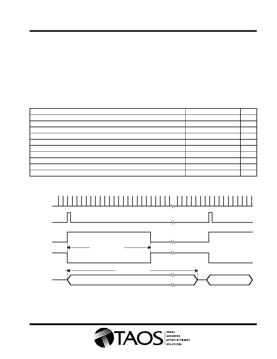
ŒŒŒŒŒŒŒŒŒŒŒŒŒŒŒŒŒŒŒŒ
ŒŒŒŒŒŒŒŒŒŒŒŒŒŒŒŒŒŒŒŒ
ŒŒŒŒŒŒŒŒ
ŒŒŒŒŒŒŒŒ
18 Clock Cycles
103 Clock Cycles
CLK
SI
AO
Internal
Reset
Integration
Hi-Z
Hi-Z
Not Integrating
Integrating
Figure 1. Timing Waveforms
TSL1301
102
◊
1 LINEAR SENSOR ARRAY WITH HOLD
TAOS006B ≠ JUNE 2001
4
www.taosinc.com
t
t
Copyright
E
2001, TAOS Inc.
Electrical Characteristics at f
clock
= 200 kHz, V
DD
= 5 V, T
A
= 25
∞
C,
p
= 565 nm, t
int
= 5 ms,
R
L
= 330
, E
e
= 800 nW/cm
2
(unless otherwise noted) (see Note 2)
PARAMETER
TEST CONDITIONS
MIN
TYP
MAX
UNIT
Analog output voltage (white, average over 102 pixels)
1.6
2
2.4
V
Analog output voltage (dark, average over 102 pixels)
E
e
= 0
0
0.3
0.4
V
PRNU
Pixel response nonuniformity
Pixels 2≠101, See Note 3
±
10%
Nonlinearity of analog output voltage
See Note 4
±
0.5%
FS
Output noise voltage
E
e
= 0, See Note 5
3
mVrms
Saturation exposure
See Note 6
5.45
7
nJ/cm
2
Analog output saturation voltage
3
3.5
V
DSNU
Dark signal nonuniformity
All pixels,
See Note 7
E
e
= 0
0.04
0.12
V
IL
Image lag
See Note 8
1%
I
DD
Supply current
2.5
4
mA
I
IH
High-level input current
V
I
= V
DD
10
µ
A
I
IL
Low-level input current
V
I
= 0
10
µ
A
C
i
Input capacitance
5
pF
NOTES: 2. Clock duty cycle is assumed to be 50%.
3. PRNU is the maximum difference between the voltage from any single pixel and the average output voltage from all pixels of the
device under test when the array is uniformly illuminated.
4. Nonlinearity is defined as the maximum deviation from a best-fit straight line over the dark-to-white irradiance levels, as a percent
of analog output voltage (white).
5. RMS noise is the standard deviation of a single-pixel output under constant illumination as observed over a 5-second period.
6. Minimum saturation exposure is calculated using the maximum responsivity and minimum output saturation voltage figures.
7. DNSU is the difference between the maximum and minimum of dark-current voltage.
8. Image lag is a residual signal left in a pixel from a previous exposure. It is defined as a percent of white-level signal remaining after
a pixel is exposed to a white condition followed by a dark condition:
IL
+
V
AO
≠V
AO(dark)
V
AO(white
)
*
V
AO(dark)
100

TSL1301
102
◊
1 LINEAR SENSOR ARRAY WITH HOLD
TAOS006B ≠ JUNE 2001
5
www.taosinc.com
t
t
Copyright
E
2001, TAOS Inc.
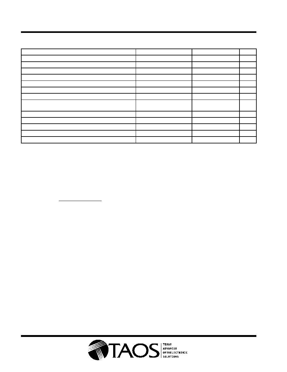
Operating Characteristics over recommended ranges of supply voltage and operating free-air
temperature (see Figure 2)
PARAMETER
TEST CONDITIONS
MIN
TYP
MAX
UNIT
t
w(H)
Clock pulse duration (high)
50
ns
t
w(L)
Clock pulse duration (low)
50
ns
t
s
Analog output settling time to
±
1%
R
L
= 330
,
C
L
= 50 pF
350
ns
50%
AO
SI
CLK
Pixel 102
t
s
0 V
0 V
5 V
2.5 V
t
h(SI)
5 V
t
su(SI)
t
w
1
2
102
103
t
s
Pixel 1
Figure 2. Operational Waveforms
TYPICAL CHARACTERISTICS
0.4
0
300
500
700
900
0.6
0.8
PHOTODIODE SPECTRAL RESPONSIVITY
0.2
≠ Wavelength ≠ nm
Normalized Responsivity
T
A
= 25
∞
C
1
1100
400
600
800
1000
Figure 3