 | –≠–ª–µ–∫—Ç—Ä–æ–Ω–Ω—ã–π –∫–æ–º–ø–æ–Ω–µ–Ω—Ç: TSL210 | –°–∫–∞—á–∞—Ç—å:  PDF PDF  ZIP ZIP |
TSL210
640
◊
1 LINEAR SENSOR ARRAY
TAOS039 ≠ AUGUST 2002
1
The
LUMENOLOGY
r
Company
t
t
Copyright
E
2002, TAOS Inc.
www.taosinc.com
D
640
◊
1 Sensor-Element Organization
D
200 Dots-Per-Inch (DPI) Sensor Pitch
D
High Linearity and Uniformity
D
Wide Dynamic Range . . . 2000:1 (66 dB)
D
Output Referenced to Ground
D
Low Image Lag . . . 0.5% Typ
D
Operation to 5 MHz
D
Single 5-V Supply
Description
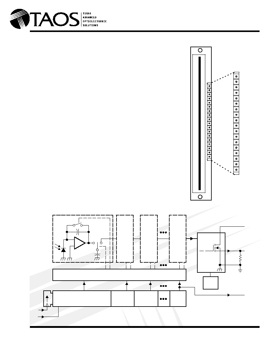
The TSL210 linear sensor array consists of five
sections of 128 photodiodes, each with
associated
charge amplifier circuitry, running from
a common clock. These sections can be
connected to form a contiguous 640
◊
1 pixel
array. Device pixels measure 120
µ
m (H) by
70
µ
m (W) with 125-
µ
m center-to-center pixel
spacing. Operation is simplified by internal logic
that requires only a serial input (SI1 through SI5)
for each section and a common clock for the five
sections.
The device is intended for use in a wide variety of
applications including contact imaging, mark and
code reading, bar-code reading, edge detection
and positioning, OCR, level detection, and linear
and rotational encoding.
Functional Block Diagram (each section)
SI
CLK
128-Bit Shift Register
Q128
Switch Control Logic
Integrator
Reset
_
+
Pixel 1
Pixel
2
Pixel
128
Pixel
3
Sample/
Output
Analog
Bus
Output
Amplifier
Gain
Trim
Q3
Q2
Q1
V
DD
R
L
(External
330
W
Load)
AO
SO
GND
t
t
Texas Advanced Optoelectronic Solutions Inc.
800 Jupiter Road, Suite 205
S
Plano, TX 75074
S
(972) 673-0759
PACKAGE
(TOP VIEW)
1 V
DD
2 CLK
3 SI1
4 AO1
5 SO1
6 SI2
7 AO2
8 SO2
9 GND
10 SI3
11 AO3
12 SO3
13 SI4
14 AO4
15 SO4
16 SI5
17 AO5
18 SO5
TSL210
640
◊
1 LINEAR SENSOR ARRAY
TAOS039 ≠ AUGUST 2002
2
t
t
Copyright
E
2002, TAOS Inc.
The
LUMENOLOGY
r
Company
www.taosinc.com
Terminal Functions
TERMINAL
I/O
DESCRIPTION
NAME
NO.
I/O
DESCRIPTION
AO1
4
O
Analog output of section 1.
AO2
7
O
Analog output of section 2.
AO3
11
O
Analog output of section 3.
AO4
14
O
Analog output of section 4.
AO5
17
O
Analog output of section 5.
CLK
2
I
Clock input for all sections. The clock controls the charge transfer, pixel output, and reset.
GND
9
Ground (substrate). All voltages are referenced to the substrate.
SI1
3
I
SI1 defines the start of the data out sequence for section 1.
SI2
6
I
SI2 defines the start of the data out sequence for section 2.
SI3
10
I
SI3 defines the start of the data out sequence for section 3.
SI4
13
I
SI4 defines the start of the data out sequence for section 4.
SI5
16
I
SI5 defines the start of the data out sequence for section 5.
SO1
5
O
SO1 provides the signal to drive the SI2 input in serial mode or
end of data for section 1 in parallel mode.
SO2
8
O
SO2 provides the signal to drive the SI3 input in serial mode or
end of data for section 2 in parallel mode.
SO3
12
O
SO3 provides the signal to drive the SI4 input in serial mode or
end of data for section 3 in parallel mode.
SO4
15
O
SO4 provides the signal to drive the SI5 input in serial mode or
end of data for section 4 in parallel mode.
SO5
18
O
SO5 provides the signal to drive the SI input of another device for cascading or as an
end of data indication.
VDD
1
Supply voltage for both analog and digital circuits.
Detailed Description
The device consists of five sections of 128 photodiodes (called pixels -- 640 total in the device) arranged in a
linear array. Each section has its own signal input and output lines, and all five sections are connected to a
common clock line. Light energy impinging on a pixel generates photocurrent that is then integrated by the active
integration circuitry associated with that pixel.
During the integration period, a sampling capacitor connects to the output of the integrator through an analog
switch. The amount of charge accumulated at each pixel is directly proportional to the light intensity on that pixel
and the integration time. The voltage output developed for each pixel is according to the following relationship:
V
out
= V
drk
+ (R
e
) (E
e
) (t
int
)
where:
V
out
is the analog output voltage for white condition
V
drk
is the analog output voltage for dark condition
R
e
is the device responsivity for a given wavelength of light given in V/(
µ
J/cm
2
)
E
e
is the incident irradiance in
µ
W/cm
2
t
int
is integration time in seconds

TSL210
640
◊
1 LINEAR SENSOR ARRAY
TAOS039 ≠ AUGUST 2002
3
The
LUMENOLOGY
r
Company
t
t
Copyright
E
2002, TAOS Inc.
www.taosinc.com
The output and reset of the integrators in each section are controlled by a 128-bit shift register and reset logic.
An output cycle is initiated by clocking in a logic 1 on SI. As the SI pulse is clocked through the shift register,
the charge stored on the sampling capacitors of each pixel is sequentially connected to a charge-coupled output
amplifier that generates a voltage on analog output AO (given above). After being read, the pixel integrator is
then reset, and the next integration period begins for that pixel. On the 129
th
clock rising edge, the SO pulse
is clocked out on SO signifying the end of the read cycle. The section is then ready for another read cycle. The
SO of each section can be connected to SI on the next section in the array (Figure 4). SO can be used to signify
the read is complete.
AO is driven by a source follower that requires an external pulldown resistor (330-
typical). The output is
nominally 0 V for no light input, 2 V for normal white-level, and 3.4 V for saturation light level. When the device
is not in the output phase, AO is in a high impedance state.
A 0.1
µ
F bypass capacitor should be connected between V
DD
and ground as close as possible to the device.

TSL210
640
◊
1 LINEAR SENSOR ARRAY
TAOS039 ≠ AUGUST 2002
4
t
t
Copyright
E
2002, TAOS Inc.
The
LUMENOLOGY
r
Company
www.taosinc.com
Absolute Maximum Ratings
Supply voltage range, V
DD
≠0.3 V to 6 V
. . . . . . . . . . . . . . . . . . . . . . . . . . . . . . . . . . . . . . . . . . . . . . . . . . . . . . . . . . .
Input voltage range, V
I
≠0.3 V to V
DD
+ 0.3V
. . . . . . . . . . . . . . . . . . . . . . . . . . . . . . . . . . . . . . . . . . . . . . . . . . . . . .
Input clamp current, I
IK
(V
I
< 0 or V
I
> V
DD
)
≠20 mA to 20 mA
. . . . . . . . . . . . . . . . . . . . . . . . . . . . . . . . . . . . . . . .
Output clamp current, I
OK
(V
O
< 0 or V
O
> V
DD
)
≠25 mA to 25 mA
. . . . . . . . . . . . . . . . . . . . . . . . . . . . . . . . . . . .
Voltage range applied to any output in the high impedance or
power-off state, V
O
≠0.3 V to V
DD
+ 0.3V
. . . . . . . . . . . . . . . . . . . . . . . . . . . . . . . . . . . . . . . . . . . . . . . . . . .
Continuous output current, I
O
(V
O
= 0 to V
DD
)
≠25 mA to 25 mA
. . . . . . . . . . . . . . . . . . . . . . . . . . . . . . . . . . . . . .
Continuous current through V
DD
or GND
≠100 mA to 100 mA
. . . . . . . . . . . . . . . . . . . . . . . . . . . . . . . . . . . . . . .
Analog output current range, I
O
≠25 mA to 25 mA
. . . . . . . . . . . . . . . . . . . . . . . . . . . . . . . . . . . . . . . . . . . . . . . . . .
Operating free-air temperature range, T
A
≠25
∞
C to 85
∞
C
. . . . . . . . . . . . . . . . . . . . . . . . . . . . . . . . . . . . . . . . . . . .
Storage temperature range, T
stg
≠25
∞
C to 85
∞
C
. . . . . . . . . . . . . . . . . . . . . . . . . . . . . . . . . . . . . . . . . . . . . . . . . . . .
Lead temperature on connection pad for 10 seconds
260
∞
C
. . . . . . . . . . . . . . . . . . . . . . . . . . . . . . . . . . . . . . . . .
ESD tolerance, human body model
2000 V
. . . . . . . . . . . . . . . . . . . . . . . . . . . . . . . . . . . . . . . . . . . . . . . . . . . . . . . .
Stresses beyond those listed under "Absolute Maximum Ratings" may cause permanent damage to the device. These are stress ratings only, and
functional operation of the device at these or any other conditions beyond those indicated under "Recommended Operating Conditions" is not
implied. Exposure to absolute-maximum-rated conditions for extended periods may affect device reliability.
Recommended Operating Conditions (see Figure 1 and Figure 2)
MIN
NOM
MAX
UNIT
Supply voltage, V
DD
4.5
5
5.5
V
Input voltage, V
I
0
V
DD
V
High-level input voltage, V
IH
2
V
DD
V
Low-level input voltage, V
IL
0
0.8
V
Wavelength of light source,
400
1000
nm
Clock frequency, f
clock
5
5000
kHz
Sensor integration time, serial, t
int
0.128
100
ms
Sensor integration time, parallel, t
int
0.026
100
ms
Load capacitance, C
L
330
pF
Load resistance, R
L
300
4700
Operating free-air temperature, T
A
0
70
∞
C
NOTE 1: SI must go low before the rising edge of the next clock pulse.
TSL210
640
◊
1 LINEAR SENSOR ARRAY
TAOS039 ≠ AUGUST 2002
5
The
LUMENOLOGY
r
Company
t
t
Copyright
E
2002, TAOS Inc.
www.taosinc.com
Electrical Characteristics at f
clock
= 200 kHz, V
DD
= 5 V, T
A
= 25
∞
C,
p
= 640 nm, t
int
= 5 ms,
R
L
= 330
, E
e
= 18
µ
W/cm
2
(unless otherwise noted) (see Note 3)
PARAMETER
TEST CONDITIONS
MIN
TYP
MAX
UNIT
V
OUT
Analog output voltage (white, average over 640 pixels)
See Note 2
1.6
2
2.4
V
V
DRK
Analog output voltage (dark, average over 640 pixels)
E
e
= 0
0
0.05
0.15
V
PRNU
Pixel response nonuniformity
See Note 4
±
20
%
Nonlinearity of analog output voltage
See Note 5
±
0.4%
FS
Output noise voltage
See Note 6
1
mVrms
R
e
Responsivity
16
22
28
V/
(µ
J/
cm
2
)
SE
Saturation exposure
See Note 7
155
nJ/cm
2
V
SAT
Analog output saturation voltage
2.5
3.4
V
DSNU
Dark signal nonuniformity
All pixels, E
e
= 0, See Note 8
0.04
0.12
V
IL
Image lag
See Note 9
0.5
%
I
DD
Supply current
125
160
mA
I
IH
High-level input current
V
I
= V
DD
10
µ
A
I
IL
Low-level input current
V
I
= 0
10
µ
A
V
O
High level output voltage SO1
SO5
I
O
= 50
µ
A
4.5
4.95
V
V
OH
High-level output voltage, SO1 ≠ SO5
I
O
= 4 mA
4.6
V
V
O
Low level output voltage SO1
SO5
I
O
= 50
µ
A
0.01
0.1
V
V
OL
Low-level output voltage, SO1 ≠ SO5
I
O
= 4 mA
0.4
V
C
i(SI)
Input capacitance, SI
20
pF
C
i(CLK)
Input capacitance, CLK
50
pF
NOTES: 2. The array is uniformly illuminated with a diffused LED source having a peak wavelength of 640 nm.
3. Clock duty cycle is assumed to be 50%.
4. PRNU is the maximum difference between the voltage from any single pixel and the average output voltage from all pixels of the
device under test when the array is uniformly illuminated.
5. Nonlinearity is defined as the maximum deviation from a best-fit straight line over the dark-to-white irradiance levels, as a percent
of analog output voltage (white).
6. RMS noise is the standard deviation of a single-pixel output under constant illumination as observed over a 5-second period.
7. Minimum saturation exposure is calculated using the minimum V
sat
, the maximum V
drk
, and the maximum R
e
.
8. DSNU is the difference between the maximum and minimum output voltage in the absence of illumination.
9. Image lag is a residual signal left in a pixel from a previous exposure. It is defined as a percent of white-level signal remaining after
a pixel is exposed to a white condition followed by a dark condition:
IL
+
V
out (IL)
*
V
drk
V
out (white)
*
V
drk
100
Timing Requirements (see Figure 1 and Figure 2)
MIN
NOM
MAX
UNIT
t
su(SI)
Setup time, serial input (see Note 10)
20
ns
t
h(SI)
Hold time, serial input (see Note 10 and Note 11)
0
ns
t
w
Pulse duration, clock high or low
50
ns
t
r
, t
f
Input transition (rise and fall) time
0
500
ns
NOTES: 10. Input pulses have the following characteristics: t
r
= 6 ns, t
f
= 6 ns.
11. SI must go low before the rising edge of the next clock pulse.