TSL257
HIGH SENSITIVITY
LIGHT TO VOLTAGE CONVERTER
TAOS023A ≠ JULY 2000
1
www.taosinc.com
t
t
Copyright
E
2001, TAOS Inc.
D
Converts Light Intensity to Output Voltage
D
Monolithic Silicon IC Containing
Photodiode, Operational Amplifier, and
Feedback Components
D
High Sensitivity
D
Single Voltage Supply Operation (2.7 V to
5.5 V)
D
Low Noise (200
µ
Vrms Typ to 1 kHz)
D
Rail-to-Rail Output
D
High Power-Supply Rejection (35 dB at
1 kHz)
D
Compact 3-Leaded Plastic Package
Description
The TSL257 is a high-sensitivity low-noise light-to-voltage optical converter that combines a photodiode and
a transimpedance amplifier on a single monolithic CMOS integrated circuit. Output voltage is directly
proportional to light intensity (irradiance) on the photodiode. The TSL257 has a transimpedance gain of 320 M
.
The device has improved offset voltage stability and low power consumption and is supplied in a 3-lead clear
plastic sidelooker package with an integral lens.
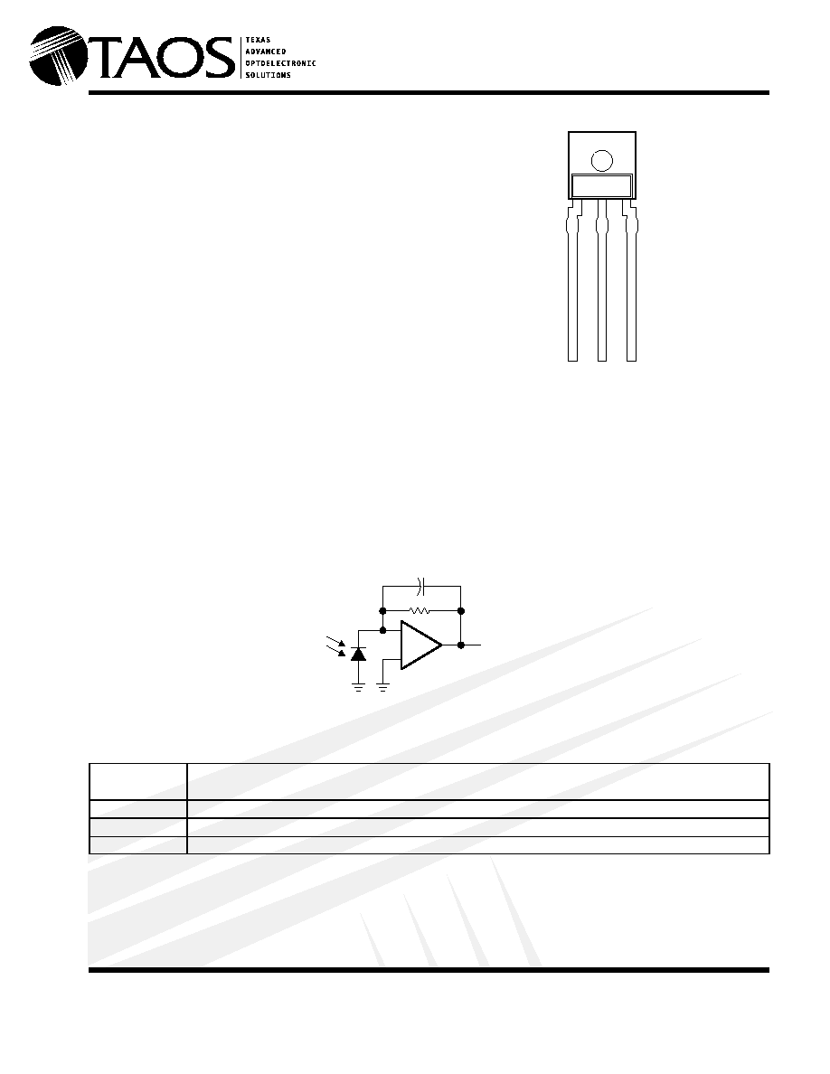
Functional Block Diagram
Voltage
Output
+
≠
Terminal Functions
TERMINAL
DESCRIPTION
NAME
NO.
DESCRIPTION
GND
1
Ground (substrate). All voltages are referenced to GND.
OUT
3
Output voltage
V
DD
2
Supply voltage
t
t
Texas Advanced Optoelectronic Solutions Inc.
800 Jupiter Road, Suite 205
S
Plano, TX 75074
S
(972) 673-0759
3
2
1
OUT
V
DD
GND
PACKAGE
(FRONT VIEW)

TSL257
HIGH SENSITIVITY
LIGHT TO VOLTAGE CONVERTER
TAOS023A ≠ JULY 2000
2
www.taosinc.com
t
t
Copyright
E
2001, TAOS Inc.
Absolute Maximum Ratings over operating free-air temperature range (unless otherwise noted)
Supply voltage, V
DD
(see Note 1)
6 V
. . . . . . . . . . . . . . . . . . . . . . . . . . . . . . . . . . . . . . . . . . . . . . . . . . . . . . . . . . . .
Output current, I
O
±
10 mA
. . . . . . . . . . . . . . . . . . . . . . . . . . . . . . . . . . . . . . . . . . . . . . . . . . . . . . . . . . . . . . . . . . . . . .
Duration of short-circuit current at (or below) 25
∞
C 5
s
. . . . . . . . . . . . . . . . . . . . . . . . . . . . . . . . . . . . . . . . . . . . . .
Operating free-air temperature range, T
A
≠25
∞
C to 85
∞
C
. . . . . . . . . . . . . . . . . . . . . . . . . . . . . . . . . . . . . . . . . . . .
Storage temperature range, T
stg
≠25
∞
C to 85
∞
C
. . . . . . . . . . . . . . . . . . . . . . . . . . . . . . . . . . . . . . . . . . . . . . . . . . . .
Lead temperature 1,6 mm (1/16 inch) from case for 10 seconds
240
∞
C
. . . . . . . . . . . . . . . . . . . . . . . . . . . . . . .
Stresses beyond those listed under "absolute maximum ratings" may cause permanent damage to the device. These are stress ratings only, and
functional operation of the device at these or any other conditions beyond those indicated under "recommended operating conditions" is not
implied. Exposure to absolute-maximum-rated conditions for extended periods may affect device reliability.
NOTE 1: All voltages are with respect to GND.
Recommended Operating Conditions
MIN
MAX
UNIT
Supply voltage, V
DD
2.7
5.5
V
Operating free-air temperature, T
A
0
70
∞
C
Electrical Characteristics at V
DD
= 5 V, T
A
= 25
∞
C,
p
= 470 nm, R
L
= 10 k
(unless otherwise noted)
(see Notes 2 and 3)
PARAMETER
TEST CONDITIONS
MIN
TYP
MAX
UNIT
V
D
Dark voltage
E
e
= 0
0
15
mV
V
Maximum output voltage swing
V
DD
= 4.5 V,
No Load
4.49
V
V
OM
Maximum output voltage swing
V
DD
= 4.5 V,
R
L
= 10 k
4
4.2
V
V
O
Output voltage
E
e
= 1.54
µ
W/cm
2
,
p
= 470 nm, Note 5
1.6
2
2.4
V
VD
Temperature coefficient of dark voltage (V
D
)
T
A
= 0
∞
C to 70
∞
C
≠15
µ
V/
∞
C
p
= 428 nm, see Notes 4 and 8
1.18
N
Irradiance responsivity
p
= 470 nm, see Notes 5 and 8
1.30
V/( W/cm
2
)
N
e
Irradiance responsivity
p
= 565 nm, see Notes 6 and 8
1.58
V/(
µ
W/cm
2
)
p
= 645 nm, see Notes 7 and 8
1.68
PSRR
Power supply rejection ratio
f
ac
= 100 Hz, see Note 9
55
dB
y
j
f
ac
= 1 kHz, see Note 9
35
dB
I
DD
Supply current
E
e
= 1.54
µ
W/cm
2
,
p
= 470 nm, Note 5
1.9
3.5
mA
NOTES:
2. Measured with R
L
= 10 k
between output and ground.
3. Optical measurements are made using small-angle incident radiation from a light-emitting diode (LED) optical source.
4. The input irradiance is supplied by a GaN/SiC light-emitting diode with the following characteristics: peak wavelength
p
= 428 nm,
spectral halfwidth
Ω
= 65 nm.
5. The input irradiance is supplied by an InGaN light-emitting diode with the following characteristics: peak wavelength
p
= 470 nm,
spectral halfwidth
Ω
= 35 nm.
6. The input irradiance is supplied by a GaP light-emitting diode with the following characteristics: peak wavelength
p
= 565 nm,
spectral halfwidth
Ω
= 28 nm.
7. The input irradiance is supplied by an AlGaAs light-emitting diode with the following characteristics: peak wavelength
p
= 645 nm,
spectral halfwidth
Ω
= 25 nm.
8. Irradiance responsivity is characterized over the range V
O
= 0.1 V to 4.5 V. The best-fit straight line of Output Voltage V
O
versus
Irradiance E
e
over this range will typically have a positive extrapolated V
O
value for E
e
= 0.
9. Power supply rejection ratio PSRR is defined as 20 log (
V
DD
(f)/
V
O
(f)) with V
DD
(f = 0) = 5 V and V
O
(f = 0) = 2 V.
TSL257
HIGH SENSITIVITY
LIGHT TO VOLTAGE CONVERTER
TAOS023A ≠ JULY 2000
3
www.taosinc.com
t
t
Copyright
E
2001, TAOS Inc.
Switching Characteristics at V
DD
= 5 V, T
A
= 25
∞
C,
p
= 470 nm, R
L
= 10 k
(unless otherwise noted)
PARAMETER
TEST CONDITIONS
MIN
TYP
MAX
UNIT
t
r
Output pulse rise time, 10% to 90% of final value
See Note 10 and Figure 1
160
250
µ
s
t
f
Output pulse fall time, 10% to 90% of final value
See Note 10 and Figure 1
150
250
µ
s
t
s
Output settling time to 1% of final value
See Note 10 and Figure 1
330
µ
s
Integrated noise voltage
f = dc to 1 kHz
E
e
= 0
200
µ
Vrms
f = 10 Hz
E
e
= 0
6
V
n
Output noise voltage, rms
f = 100 Hz
E
e
= 0
6
µ
V/
Hz rms
n
g ,
f = 1 kHz
E
e
= 0
7
µ
NOTE 10: Switching characteristics apply over the range V
O
= 0.1 V to 4.5 V.
PARAMETER MEASUREMENT INFORMATION
VOLTAGE WAVEFORM
TEST CIRCUIT
Input
E
e
10%
90%
Output
(see Note B)
t
r
TSL257
R
L
V
DD
2
1
3
+
≠
Output
Pulse
Generator
LED
(see Note A)
t
f
90%
10%
NOTES: A. The input irradiance is supplied by a pulsed InGaN light-emitting diode with the following characteristics:
p
= 470 nm,
t
r
< 1
µ
s, t
f
< 1
µ
s.
B. The output waveform is monitored on an oscilloscope with the following characteristics: t
r
< 100 ns, Z
i
1 M
, C
i
20 pF.
Figure 1. Switching Times

TSL257
HIGH SENSITIVITY
LIGHT TO VOLTAGE CONVERTER
TAOS023A ≠ JULY 2000
5
www.taosinc.com
t
t
Copyright
E
2001, TAOS Inc.
MECHANICAL DATA
The TSL257 is implemented in a clear 3-leaded package with a molded focusing lens.
0.072 (1,84)
0.189 (4,80)
0.630 (16,00)
0.173 (4,40)
0.029 (0,75)
0.057 (1,44)
0.018 (0,45)
0.531 (13,50)
0.027 (0,70)
0.079 (2,00)
0.071 (1,80)
0.110 (2,80)
0.039 (1,00)
0.165 (4,20)
0.150 (3,80)
0.189 (4,80)
0.173 (4,40)
0.026 (0,65)
0.016 (0,40)
0.032 (0,80)
0.071 (1,8)
0.079 (2,00)
0.016 (0,40)
R 0.035 (0,90)
0.079 (2,00)
0.018 (0,45)
0.102 (2,6)
Figure 6. Package Configuration
NOTES: A. All linear dimensions are in inches (millimeters).
B. This drawing is subject to change without notice.
C. All dimensions apply before solder dip.
D. Package body is a clear nonfilled optically transparent material
E. Index of refraction of clear plastic is 1.55.